


Si53xx-RM
Rev. 0.5 117
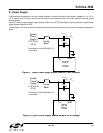
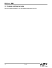
9. Power Supply
These devices incorporate an on-chip voltage regulator to power the device from supply voltages of 1.8, 2.5, or
3.3 V. Internal core circuitry is driven from the output of this regulator while I/O circuitry uses the external supply
voltage directly.
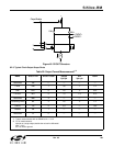
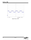
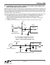
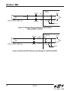
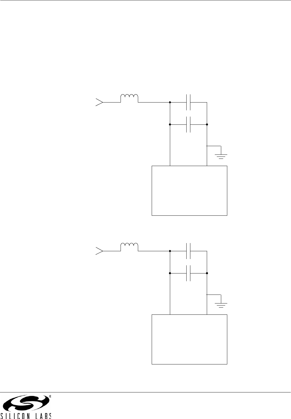
Figure 57 shows a typical power supply bypass network for the TQFP packages. Figure 58 shows a typical power
supply bypass network for QFN.
In both cases, the center ground pad under the device must be electrically and thermally connected to the ground
plane.
Figure 57. Typical Power Supply Bypass Network (TQFP Package)
Figure 58. Typical Power Supply Bypass Network (QFN Package)
TQFP
PKG
V
DD
GND
C
1
– C
8
C
9
Ferrite
Bead
System
Power
Supply
(1.8, 2.5 or
3.3 V)
0.1 uF
1.0 uF
Ferrite bead is Venkel BC1206-471H
or equivalent.
QFN
PKG
V
DD
GND
C
1
– C
3
C
4
Ferrite
Bead
0.1 uF
1.0 uF
System
Power
Supply
(1.8, 2.5, or
3.3 V)
Ferrite bead is Venkel BC1206-471H
or equivalent.