


Si53xx-RM
Rev. 0.5 169
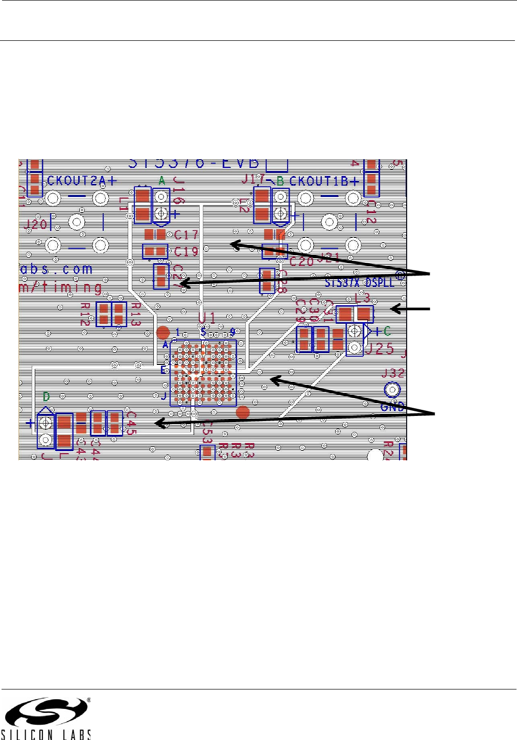
APPENDIX I—Si5374 AND Si5375 PCB LAYOUT RECOMMENDATIONS
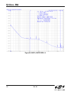
The following is a set of recommendations and guidelines for printed circuit board layout with the Si5374 and
Si5374 devices. Because the four DSPLLs are in close physical and electrical proximity to one another, PCB layout
is critical to achieving the highest levels of jitter performance. The following images were taken from the Si537x-
EVB (evaluation board) layout. For more details about this board, refer to the Si537x-EVB Evaluation Board User's
Guide.
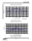
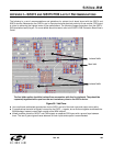
Figure 95. Vdd Plane
Use a solid and undisturbed ground plane for the Si537x and all of the clock input and output return paths.
For applications that wish to logically connect the four RSTL_x signals, do not tie them together underneath the
BGA package. Instead connect them outside of the BGA footprint.
Where possible, place the CKOUT and CKIN signals on separate PCB layers with a ground layer between
them. The use of ground guard traces between all clock inputs and outputs is recommended.
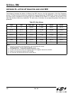
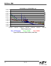
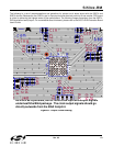
IsolatedVdd’s
MainVdd
IsolatedVdd’s
ThefourVddsuppliesshouldbeisolat edfromoneanotherwithfou rferritebeads.Theyshouldbe
separatelybypa ssedwithcapacitorsthatarelocatedveryclosetotheSi537xdevice.