


Si53xx-RM
Rev. 0.5 29
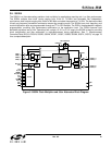
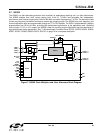
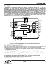
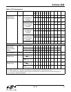
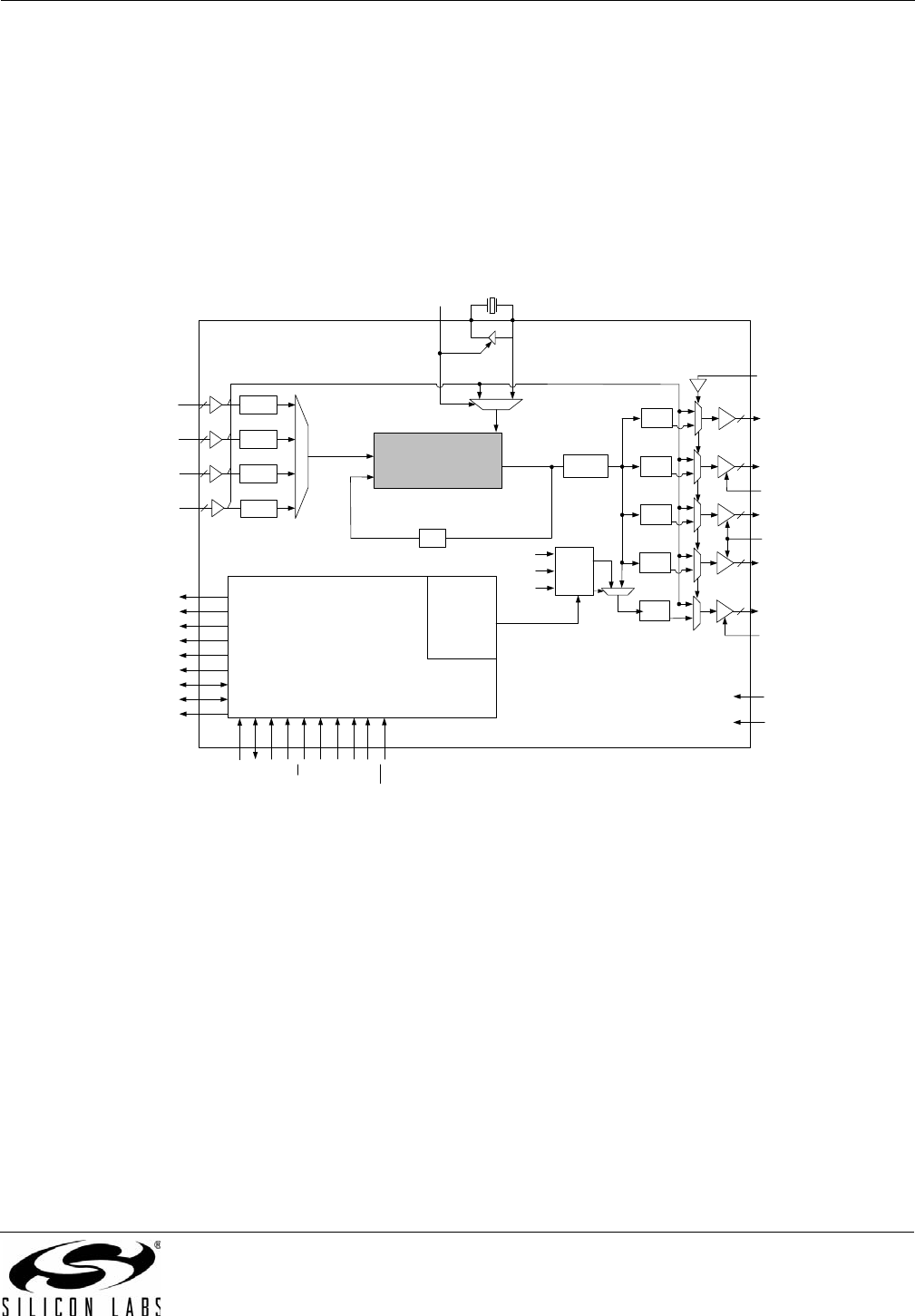
3.13. Si5369
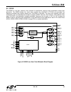
The Si5369 is a jitter-attenuating precision clock multiplier for applications requiring sub 1 ps rms jitter
performance. The Si5369 accepts four clock inputs ranging from 2 kHz to 710 MHz and generates five
independent, synchronous clock outputs ranging from 2 kHz to 945 MHz and select frequencies to 1.4 GHz. The
device provides virtually any frequency translation combination across this operating range. The Si5369 input clock
frequency and clock multiplication ratio are programmable through an I
2
C or SPI interface. The DSPLL loop
bandwidth is digitally programmable, providing loop bandwidth values as low as 4 Hz. Operating from a single 1.8,
2.5, or 3.3 V supply, the Si5369 is ideal for providing clock multiplication and jitter attenuation in high performance
timing applications. See "7. Microprocessor Controlled Parts (Si5319, Si5324, Si5325, Si5326, Si5327, Si5367,
Si5368, Si5369, Si5374, Si5375)" on page 76 for a complete description.
Figure 13. Si5369 Clock Multiplier and Jitter Attenuator Block Diagram
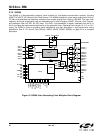
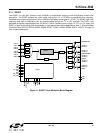
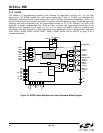
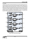
3.14. Si5374/75 Compared to Si5324/19
In general, the Si5374 can be viewed as a quad version of the Si5324 and the Si5375 can be viewed as a quad
version of the Si5319. However, there are not exactly the same. This is an overview of the differences:
1. The Si5374/75 cannot use a crystal as its OSC reference. It requires the use of a single external single-ended
or differential crystal oscillator.
2. The Si5374/75 only supports I
2
C as its serial port protocol and does not have SPI. No I
2
C address pins are
available on the Si5374/75.
3. The Si5374/75 does not provide separate INT_CK1B and CK2B pins to indicate when CKIN1 and CKIN2 do not
have valid clock inputs. Instead, the IRQ pin can be programmed to function as one pin, the other pin or both.
4. Selection of the OSC frequency is done by a register (RATE_REG), not by using the RATE pins.
5. The Si5374/75 uses a different version of DSPLLsim: Si537xDSPLLsim.
6. The Si5374/75 does not support 3.3 V operation.
C2A
CS0_C3A
C2B
CS1_C4A
INT_ALM
C1A
CKIN_1+
CKIN_1–
CKIN_2+
CKIN_2–
C3B
CKIN_3+
CKIN_3–
CKIN_4+
CKIN_4–
C1B
CKIN_3
CKIN_4
CKOUT_2
VDD
GND
CKOUT_1+
CKOUT_1–
÷ NC1
1
0
CKOUT_2+
CKOUT_2–
÷ NC2
1
0
CKOUT_3+
CKOUT_3–
÷ NC3
1
0
CKOUT_4+
CKOUT_4–
÷ NC4
1
0
2
2
2
2
2
2
2
2
f
OSC
Xtal or Refclock
RATE[1:0]
XA
XB
f
x
DSBL2/BYPASS
DSBL34
DSBL5
FSYNC
LOGIC/
ALIGN
SDA_SDO
SCL
SDI
A[1:0]
INC
DEC
FS_ALIGN
RST
CMODE
BYPASS/DSBL2
LOL
Control
÷ N3_2
÷ N3_1
FSYNC
÷ N2
÷ N3_3
÷ N3_4
CKOUT_5+
CKOUT_5–
÷ NC5
1
0
2
1
0
A[2]/SS
÷ N1_HS
DSPLL
®
f
3
3