


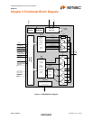
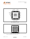
Hi-Speed USB Device PHY with UTMI Interface
Datasheet
SMSC USB3280 11 Revision 1.5 (11-15-07)
DATASHEET
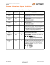
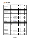
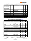
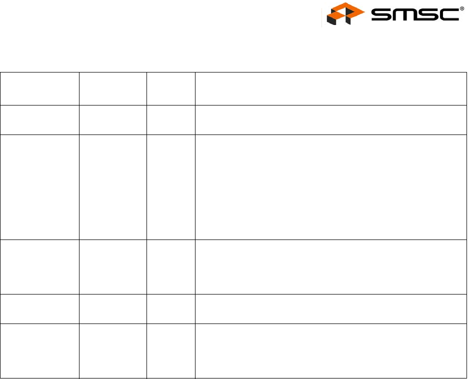
Table 4.5 Power and Ground Signals
NAME DIRECTION
ACTIVE
LEVEL DESCRIPTION
VDD3.3
(V33)
N/A N/A 3.3V Supply. Provides power for USB 2.0 Transceiver, UTMI+
Digital, Digital I/O, and Regulators.
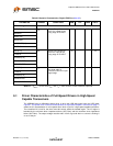
REG_EN
(REN)
Input High On-Chip 1.8V regulator enable. Connect to ground to disable
both of the on chip (VDDA1.8 and VDD1.8) regulators. When
regulators are disabled:
External 1.8V must be supplied to VDDA1.8 and VDD1.8 pins.
When the regulators are disabled, VDDA1.8 may be connected
to VDD1.8 and a bypass capacitor (0.1μF recommended)
should be connected to each pin.
The voltage at VDD3.3 must be at least 2.64V (0.8 * 3.3V)
before voltage is applied to VDDA1.8 and VDD1.8.
VDD1.8
(V18)
N/A N/A 1.8V Digital Supply. Supplied by On-Chip Regulator when
REG_EN is active. Low ESR 4.7uF minimum capacitor
requirement when using internal regulators. Do not connect
VDD1.8 to VDDA1.8 when using internal regulators. When the
regulators are disabled, VDD1.8 may be connected to VDD1.8A.
VSS
(GND)
N/A N/A Common Ground.
VDDA1.8
(V18A)
N/A N/A 1.8V Analog Supply. Supplied by On-Chip Regulator when
REG_EN is active. Low ESR 4.7uF minimum capacitor
requirement when using internal regulators. Do not connect
VDD1.8A to VDD1.8 when using internal regulators. When the
regulators are disabled, VDD1.8A may be connected to VDD1.8.