


Hi-Speed USB Device PHY with UTMI Interface
Datasheet
SMSC USB3280 15 Revision 1.5 (11-15-07)
DATASHEET
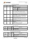
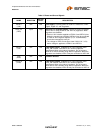
Note 6.3 V
DD3.3
= 3.0 to 3.6V; V
SS
= 0V; T
A
= -40
o
C to 85
o
C; unless otherwise specified.
Note 6.4 V
DD3.3
= 3.0 to 3.6V; V
SS
= 0V; T
A
= -40
o
C to 85
o
C; unless otherwise specified.
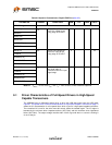
High Speed High Level
Output Voltage (DP/DM
referenced to GND)
V
HSOH
45Ω load 360 440 mV
High Speed IDLE Level
Output Voltage (DP/DM
referenced to GND)
V
OLHS
45Ω load -10 10 mV
Chirp-J Output Voltage
(Differential)
V
CHIRPJ
HS termination resistor
disabled, pull-up resistor
connected. 45Ω load.
700 1100 mV
Chirp-K Output Voltage
(Differential)
V
CHIRPK
HS termination resistor
disabled, pull-up resistor
connected. 45Ω load.
-900 -500 mV
Leakage Current
OFF-State Leakage Current I
LZ
± 1 uA
Port Capacitance
Transceiver Input Capacitance C
IN
Pin to GND 5 10 pF
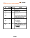
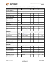
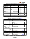
Table 6.4 Dynamic Characteristics: Analog I/O Pins (DP/DM) (Note 6.4)
PARAMETER SYMBOL CONDITIONS MIN TYP MAX UNITS
FS Output Driver Timing
Rise Time T
FSR
C
L
= 50pF; 10 to 90% of
|V
OH
- V
OL
|
420ns
Fall Time T
FFF
C
L
= 50pF; 10 to 90% of
|V
OH
- V
OL
|
420ns
Output Signal Crossover
Voltage
V
CRS
Excluding the first
transition from IDLE state
1.3 2.0 V
Differential Rise/Fall Time
Matching
FRFM Excluding the first
transition from IDLE state
90 111.1 %
HS Output Driver Timing
Differential Rise Time T
HSR
500 ps
Differential Fall Time T
HSF
500 ps
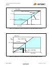
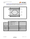
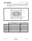
Driver Waveform
Requirements
Eye pattern of Template 1
in USB 2.0 specification
See
Figure 6.2
High Speed Mode Timing
Receiver Waveform
Requirements
Eye pattern of Template 4
in USB 2.0 specification
See
Figure 6.2
Data Source Jitter and
Receiver Jitter Tolerance
Eye pattern of Template 4
in USB 2.0 specification
See
Figure 6.2
Table 6.3 DC Electrical Characteristics: Analog I/O Pins (DP/DM) (Note 6.3) (continued)
PARAMETER SYMBOL CONDITIONS MIN TYP MAX UNITS