


Chapter 2: Installation
2-21
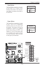
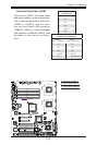
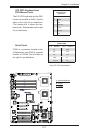
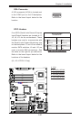
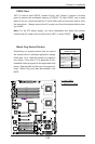
JBT1
DIMM2A
SP1
JI2C1
JI2C2
JL1
LED5
LED6
LED3
JWD1
JPG1
JPL2
JPA1
Fan 4
JD1
LED4
JWOL1
JPWF1
JAR
8-Pin PWR
I-Button
LAN
CTRL
VGA
CTRL
S I/O
SATA4
SATA3
SATA2
SATA1
SATA0
SATA5
SATA-GPIO0
Battery
SAS0
SAS1
SAS2
SAS3
SAS4
SAS5
SAS6
SAS7
PWR LED
JP1
JP2
COM2
JWOR1
JKEY1
Buzzer
BIOS
SATA-GPIO1
ITE
CTRL
LAN
CTRL
DIMM1A
DIMM2B
DIMM1B
DIMM2C
DIMM1C
LED1
SAS-GPIO0
SAS-GPIO1
24-Pin PWR
JPA2
System Status LED
Fan 1
CPU1 VRM OH LED
CPU2 VRM OH LED
Floppy
IDE
BPI
2
C
USB2/3
SMB_PS
KB/MS
COM1
VGA
FAN6
Slot4 PCI-E x4(in x8 slot)
Slot1 PCI 33MHz
SIMLC
USB0/1
LAN1
LAN2
FAN5
CPU1
CPU2
Fan 2
Fan 3
FP CTRL
USB4/5
Slot2 PCI 33MHz
Slot3 PCI 33MHz
Slot5 PCI-E x8
Slot6 PCI-E x8
Intel
5100
North Bridge
South Bridge
ICH9R
Intel
LSI
SAS
CTRL
JPL1
X7DCL-3/i
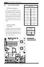
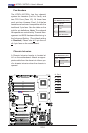
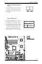
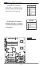
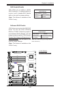
A
A. VGA
B. J7: SATA_GPIO#0
C. J8: SATA_GPIO#1
D. J9: SAS_GPIO#0
E. J10: SAS_GPIO#1
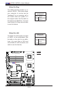
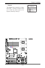
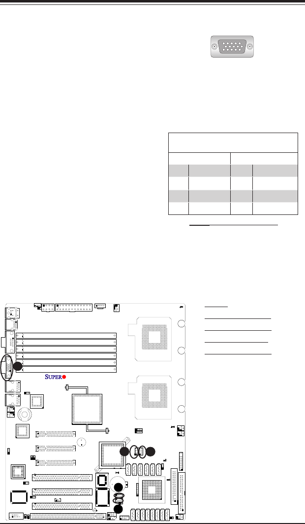
VGA Connector
A VGA connector (JVGA) is located next
to the COM1 port on the IO backplane.
Refer to the board layout below for the
location.
C
B
E
D
GPIO Headers
Four GPIO (Serial Links General Purpose
Input/Output) headers are located at J7,
J8, J9, J10 on the motherboard. These
headers are used to communicate with
the Seriel-Links System Monitoring chip
on the backplane. J7 and J8 are used to
monitor SATA activities, J9 and J10 are
used to monitor SAS connections. See
the table on the right for pin denitions.
Refer to the board layout below for the
locations of the headers.
(J9, J10: X7DCL-3 Only.)
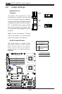
Serial-Links GPIO
PinDenitions
Pin# Denition Pin Denition
1 NC 2 NC
3 Ground 4 DATA Out
5 Load 6 Ground
7 Clock 8 NC
Note: NC= No Connections