


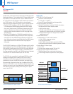
Interface Selection Guide Texas Instruments 4Q 2006
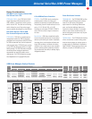
The XIO1100 is a PCI Express PHY, compliant with the PCI Express Base
Specification Revision 1.1 that interfaces the PCI Express Media Access
Layer (MAC) to a PCI Express serial link. It uses a modified version of
the “PHY Interface for the PCI Express” (PIPE) interface also referred to
as a TI-PIPE interface. The TI-PIPE interface is a pin-configurable
interface that can be configured as either a 16-bit or an 8-bit interface.
• The 16-bit TI-PIPE interface is a 125 MHz 16-bit parallel interface,
a 16 bits output bus (RXDATA) being clocked by the RXCLK output
clock, and a 16-bits Input bus (TXDATA) being clocked by the TXCLK
input clock. Both buses are clocked using Single Data Rate (SDR)
clocking in which the data transitions are on the rising-edge of the
associated clock.
• The 8-bit TI-PIPE interface is a 250 MHz 8-bit parallel interface, an
8-bit output bus (RXDATA) being clocked by the RXCLK output clock,
and an 8-bit input bus (TXDATA) being clocked by the TXCLK input
clock. Both buses are clocked using Double Data Rate (DDR) clocking
where the data transitions on both the clock’s rising-edge and
falling-edge.
The XIO1100 PHY interfaces to a 2.5Gbps PCI Express serial link with a
transmit differential pair (TXP and TXN) and a receive differential pair
(RXP and RXN). Incoming data at the XIO1100 PHY receive differential
pair (RXP and RXN) is forwarded to the MAC on the RXDATA output
bus. Data received from the MAC on the TXDATA input bus is forwarded
to the XIO1100 PHY transfer differential pair (TXP and TXN).
The XIO1100 is also responsible for handling the 8B/10B encoding/
decoding of the outgoing data. In addition, XIO1100 can recover/
interpolate the clock on the receiver side based on the transitions
guaranteed by the use of the 8B/10B mechanism and supply this to
the receive side of the data link layer logic. In addition to the TI-PIPE
Interface, the XIO1100 has some TI proprietary side-band signals some
customers may wish to use to take advantage of additional low-power
state features (for example, disabling the PLL during the L1 power
state) of the XIO1100.
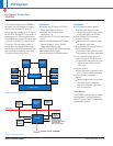
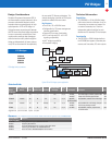
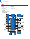
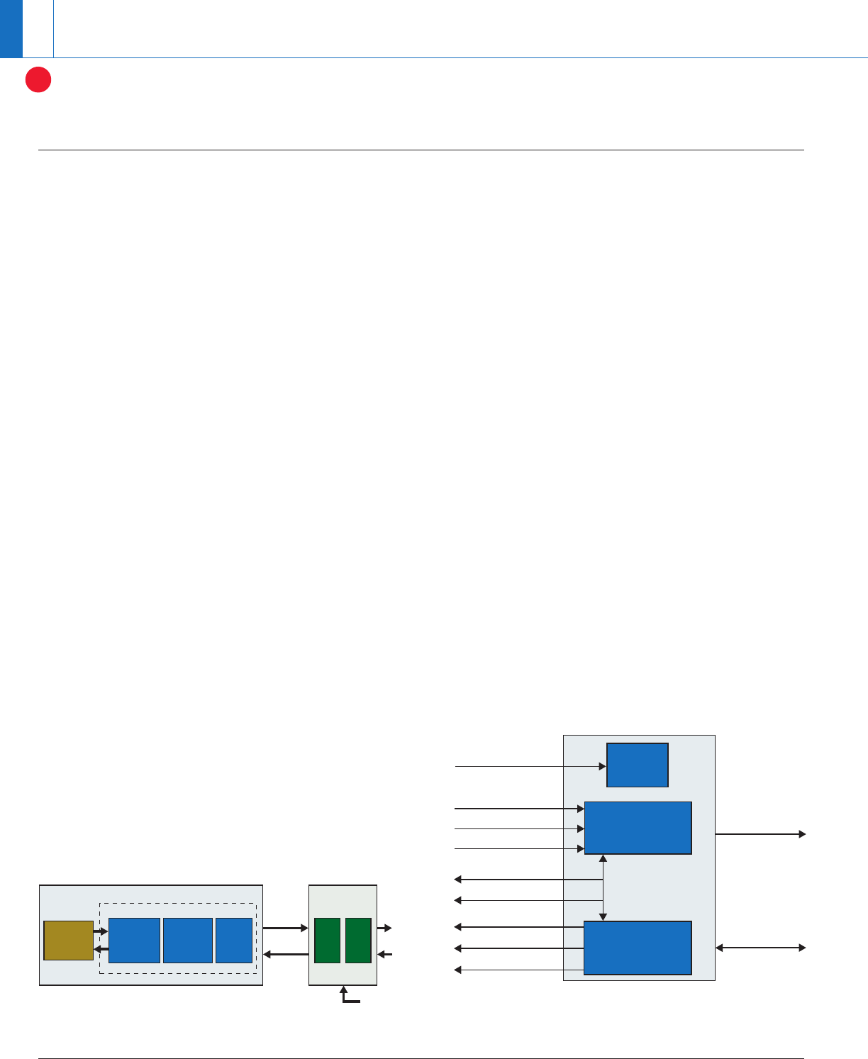
TX Block
PLL
REFCLK±
TXP/TXN
RXP/RXN
TX_DATA 16/8
TX_CLK
TX_DATAK [1:0]
RX_DATAK [1:0]
STATUS
COMMAND
RX_DATA 16/8
RX_CLK
RX Block
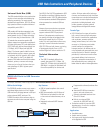
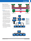
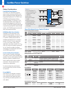
FPGA
PCIe x1 IP Core
User
Application
Layer
Transaction
Layer
Data Link
Layer
MAC
Enhanced
PIPE
TI XIO1100
2.5
Gbps
2.5
Gbps
REF CLK
PCS PMA
Key Benefits
• XIO1100 is TI’s Third-Generation PHY
••
Passed PCI SIG Workshop #49
• v1.0a and v1.1 compliant
••
Proven PCI Express Compatibility and Interoperability
• Source-Synchronous (SS) Clocking
••
Without SS clocking and running at 125 MHz the interface
must be tuned to the center capture window
• Painful and not robust
• XIO1100 is SS in BOTH RX and TX directions which makes
positioning I/O capture window easy to identify and robust
• SS approach works great from design without need for
experimental tuning
• Flexible MAC Interface
••
Selectable 8-bit or 16-bit Parallel Interface
• 16-bit: 125MHz rising-edge clocked
• Can use low-cost FPGAs
• 8-bit: 125MHz rising-and-falling edge clocked (DDR)
• No need for extra clock buffer needed to generate 250MHz
• Flexible Digital I/O Power Supply
••
1.5V or 1.8V
••
Only two supply voltages needed: 3.3V and 1.5V
• Support for two PCI Express Reference Clocks
••
100 MHz differential for normal system clock designs
••
125 MHz single-ended for asynchronous clocking designs
XIO1100 functional block diagram.
Low-cost FPGA-based PCI Express
®
solution.
PCI Express
®
32
➔
PCI Express PHY
XIO1100
G
et samples, datasheets, EVMs and app reports at:
w
ww.ti.com/sc/device/XIO1100