


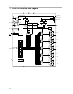
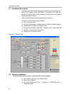
Board View and Connector Location
3-2
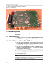
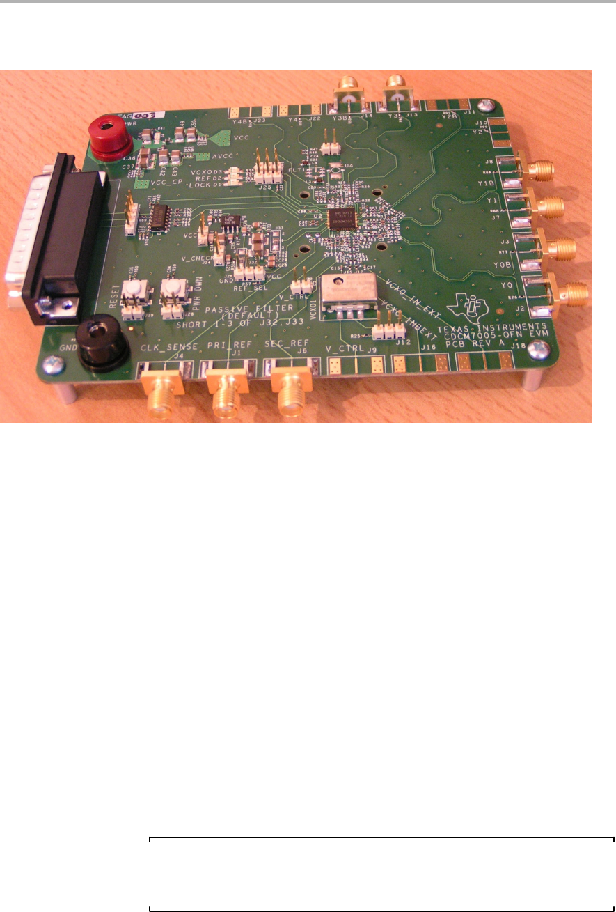
3.1 Board View and Connector Location
Figure 3−1. Board View
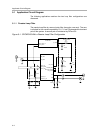
3.2 Hardware Configuration
This section describes the board configuration using on-board jumpers and
solder bridges.
3.2.1 Power Supply (P1, P2)
- Supply 3.3 V ±10% on P1 and P2 using a stabilized external power supply.
J WARNING: Never supply more than 3.6 V on P1.
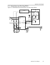
3.2.2 Onboard Switches and Indicators (SW1−SW2, D1−D4)
- Push SW1 to enter the power-down mode of the CDCM7005 device. Then
all current sources are switched off, all outputs are switched into 3-state,
and all dividers (M, N, and P) are reset to default.
- Push SW2 to enter the reset mode of the device. The charge pump (CP)
is switched to 3-state and all counters (N, M, P) are rest to zero (the initial
divider settings are maintained in SPI.
- The three status outputs of the CDCM7005 are fed to LED indicators. D1
on indicates a valid reference input clock signal. D2 is on if the VC(X)O
input clock is valid and D3 turns on if the PLL has been locked.
- D4 indicates power supply
Note:
In case of a low input impedance of the VC(X)O control voltage input, there
is a possibility D3 may not turn on to indicate locking.