


Hardware Configuration
3-3
EVM Hardware
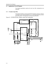
3.2.3 Programming Interfaces (J30, J31)
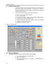
The SPI of the device is used for writing to the control register of the device.
It consists of three control lines CTRL_CLK, CTRL_DATA, and CTRL_LE.
There are four 30-bit wide RAM registers, which can be addressed by the two
LSBs of a transferred word. Every transmitted word must have 32 bits, starting
with MSB. After supplying power or activating the power-down mode, the
registers are loaded with the device default values internally (see the
CDCM7005 data sheet, SCAS793). However, if specific register settings are
required for any applications, there are two ways to program the device
externally:
- Connect the parallel port cable to the PC and EVM parallel port. This
needs control S/W (see Chapter 4).
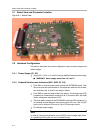
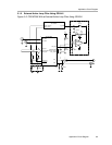
3.2.4 Loop Filter (J32−J34)
The loop filter is one of the key elements determining the loop bandwidth of
the PLL. The loop filter converts the charge pump current into the control
voltage for the voltage controlled oscillator. The phase difference between the
input clocks of the phase frequency detector determines the width of the
charge pump output current pulses. These high frequency pulses are
transformed into a voltage to control the oscillator.
Basically, three types of loop filters are implemented on the EVM.
- Passive loop filter
- External active loop filter using an external low-noise OPA.
Filter types can be selected by soldering bridges J32−J34, see Table 3−1.
Control voltage of the VC(X)O can be measured at J9 or TP1. If an external
OPA is used, it needs to be switched on by connecting J34. For example,
passive filter operation is provided when pads 1 and 3 of J33 are solder bridged
and pads 1 and 3 of J32 are solder bridged.
Default setting: Passive Loop Filter
Table 3−1. Filter Configurations
Bridge Passive Filter Active With An External OPA
J33 1−3 1−2
J34 Open Closed
J32 1−3 1−2
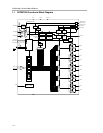
3.2.5 High-Speed Outputs and Inputs (J1−J4, J6−J11, J13, J14, J22, and J23)
The CDCM7005 drives five differential LVPECL outputs. All PECL outputs are
ac-coupled and terminated with 150 Ω to GND. This is in contrast to typical
LVPECL termination, which requires V
CC
− 2 V as termination voltage. The
reason is to simplify the power supply scheme. The device output’s trace
impedance is 50 Ω and traces are matched in length. All outputs have options
for pullup and pulldown resistors.