


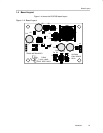


Design Procedures
2-4
2.3 Design Procedures
Detailed steps in the design of a buck-mode converter may be found in
Designing With the TL5001C PWM Controller (literature number SLVA034)
from TI. This section shows the basic steps involved in this design.
2.3.1 Duty Cycle Estimate
The duty cycle for a continuous-mode step-down converter is approximately:
D
V
O
V
d
V
I
– V
SAT
Assuming the diode or synchronous switch forward voltage V
d
= 0.12 V and
the power-switch-on voltage V
SAT
= 0.15 V, the duty cycle for V
I
= 5.5, 9, and
12 V is 0.64, 0.39, and 0.29, respectively.
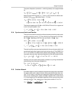
2.3.2 Output Filter
A synchronous buck converter uses a single-stage LC filter. Choose an induc-
tor to maintain continuous-mode operation down to 15 percent of the rated out-
put load:
I
O
2 0.15 I
O
2 0.15 3 0.9 A
The inductor value is:
L
V
I
– V
SAT
– V
O
D t
I
O
(12 – 0.15 – 3.3) 0.29
10 10
–6
0.9
27.6 H
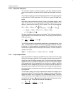
Assuming that all of the inductor ripple current flows through the capacitor and
the effective series resistance (ESR) is zero, the capacitance needed is:
C
I
O
8 f V
O
0.9
8
100 10
3
0.05
22.5 F
Assuming the capacitance is very large, the ESR needed to limit the ripple to
50 mV is:
ESR
V
O
I
O
0.05
0.9
0.056
The output filter capacitor should be rated at least ten times the calculated ca-
pacitance and 30–50 percent lower than the calculated ESR. This design used
two 100- F capacitors in parallel with a multilayer ceramic to reduce ESR.
2.3.3 Power Switch
Based on the preliminary estimate, r
DS(ON)
should be less than 0.015 V 3A
= 50 m . The IRF7406 is a 30-V p-channel MOSFET with r
DS(ON)
= 40 m