Design Procedures
2-6
2.3.6 Controller Functions
The controller functions, oscillator frequency, soft-start, dead-time-control,
short-circuit protection, and sense-divider-network are discussed in this sec-
tion.
The oscillator frequency is set by selecting the resistance value from the graph
in figure 6 of the TL5001 data sheet. For 100 kHz, a value of 90.9 k is se-
lected.
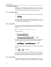
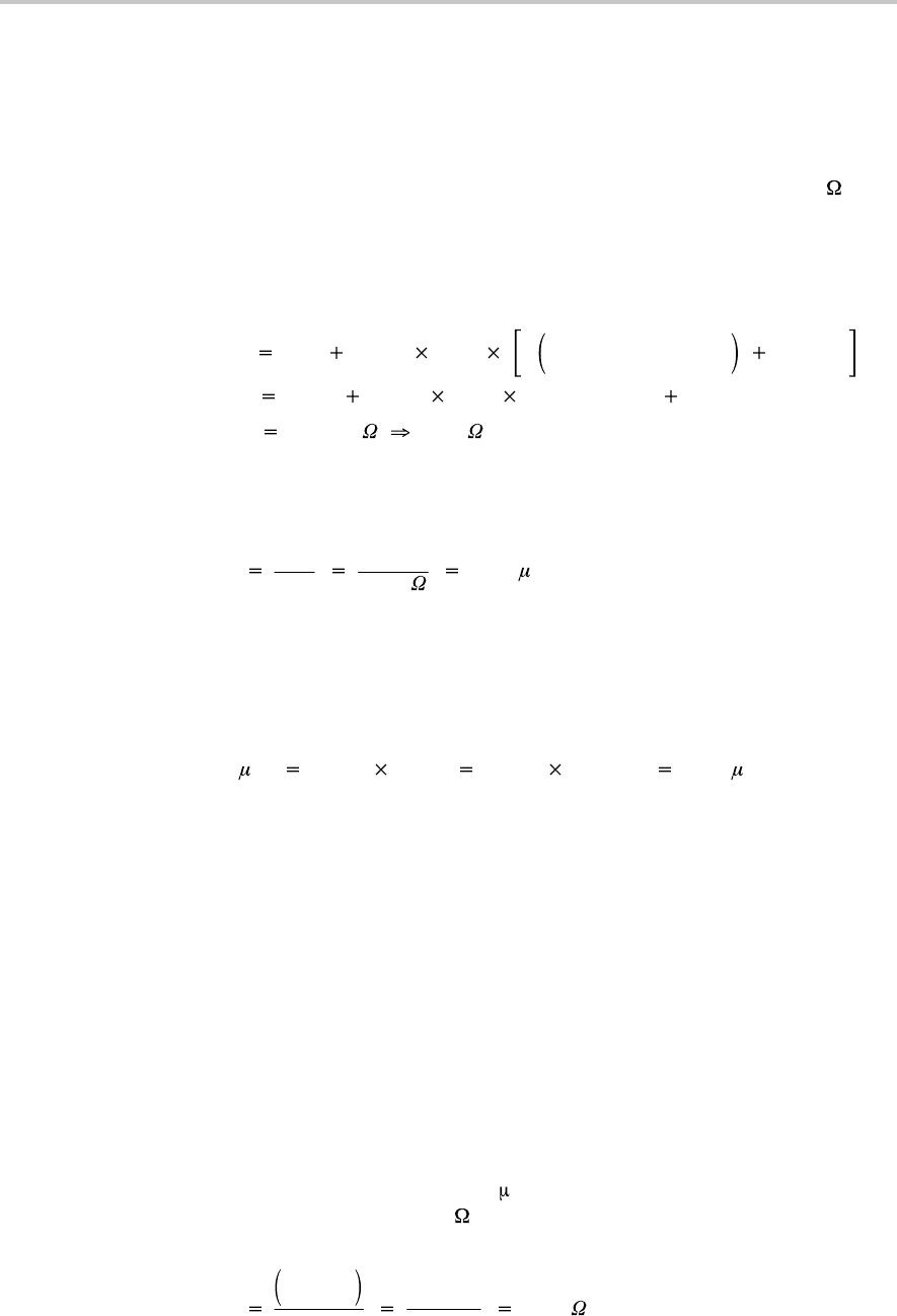
Dead-time control provides a minimum off-time for the power switch in each
cycle. Set this time by connecting a resistor between DTC and GND. For this
design, a maximum duty cycle of 100% is chosen. Then R8 is calculated as:
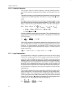
R8 (R9 1.25) 10
3
D V
O(100%)
– V
O(0%)
V
O(0%)
(90.9 1.25) 10
3
[1(1.3 – 0.65) 0.65]
119.8 K 121 k
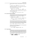
Soft-start is added to reduce power-up transients. This is implemented by ad-
ding a capacitor across the dead-time resistor. In this design, a soft-start time
of 25 ms is used:
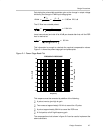
C
t
R
R
DT
0.025 s
121 k
0.21 F
The TL5001 has short circuit protection instead of a current sense circuit. If not
used, the SCP terminal must be connected to ground to allow the converter
to start up. If a timing capacitor is connected to SCP, it should have a time
constant that is greater than the soft-start time constant. This time constant is
chosen to be 75 ms:
C( F) 12.46 t
SCP
12.46 0.075 s 0.93 F
2.3.7 Loop Compensation
Loop compensation is necessary to stabilize the converter over the full range
of load, line, and gain conditions. A buck-mode converter has a two-pole LC
output filter with a 40-dB-per-decade rolloff. The total closed-loop response
needed for stability is a 20-dB-per-decade rolloff with a minimum phase margin
of 30 degrees over the full bandwidth for all conditions. In addition, sufficient
bandwidth must be designed into the circuit to assure that the converter will
have good transient response. Both of these requirements are achieved by ad-
ding compensation components around the error amplifier to modify the total
loop response.
The first step in design of the loop compensation network is the design of the
output sense divider. This sets the output voltage and the top resistor deter-
mines the relative size of the rest of the compensation design. Since the
TL5001 input bias current is 0.5 A (worst case), the divider current should be
at least 0.5 mA. Using a 1-k resistor for the bottom of the divider gives a divid-
er current of 1 mA. The top of the divider is calculated as:
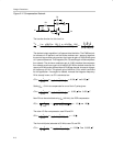
R
V
O
– 1
1 mA
(
3.3 –1
)
0.001
2.3 k


