


Design Procedures
2-5
Design Procedure
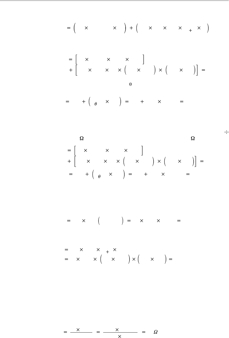
The power dissipation (conduction + switching losses) can be approximated
as:
P
D
I
2
O
r
DS(ON)
D 0.5 V
I
I
O
t
r f
f
Assuming total switching time, t
r+f
, = 100 ns, a 55°C maximum ambient tem-
perature, and r
DS(ON)
adjustment factor = 1.6, then:
P
D
3
2
(0.04 1.6) 0.64
0.5 5.5 3 0.1 10
–6
100 10
3
0.45 W
The thermal impedance for Q1 R
JA
= 90°C/W for FR-4 with 2-oz. copper and
a one-inch-square pattern, thus:
T
J
T
A
R
JA
P
D
55 (90 0.45) 96°C
2.3.4 Synchronous Switch and Rectifier
The synchronous switch calculations follow the same path as the power switch
except that the duty cycle is 1–D. Then r
DS(ON)
should be less than 0.012 V
3A = 40 m . Selecting an IRF7201 with an r
DS(ON)
= 30 m , then:
P
D
3
2
(0.03 1.6) 0.36
0.5 5.5 3 0.1 10
–6
100 10
3
0.238 W
T
J
T
A
R
JA
P
D
55 (90 0.238) 76°C
The catch rectifier serves as a backup device for the synchronous switch and
conducts during the time interval when both devices are off. The 30BQ015 is
a 3-A, 15-V rectifier in an SMC power surface-mount package. If the synchro-
nous switch were not used, the power dissipation for the catch diode would be:
P
D
I
O
V
D
1 – D
Min
3 0.7 0.71 1.491 W
However, since the catch diode actually conducts only during the deadtime
and switching time, the power dissipation is:
P
D
I
O
V
D
t
r f
f
3 0.7 0.1 10
–6
100 10
3
2.1 mW
2.3.5 Snubber Network
A snubber network is usually needed to suppress the ringing at the node where
the power switch drain, output inductor, and synchronous switch drain con-
nect. This is usually a trial-and-error sequence of steps to optimize the net-
work, but as a starting point, select a snubber capacitor with a value that is
4–10 times larger than the estimated capacitance of the synchronous switch
and catch rectifier. Then, measuring a ringing time constant of 3 ns, R is:
R
3 10
–9
C
3 10
–9
1000 10
–12
3