


© 2006 - 2008 TOSHIBA TEC CORPORATION All rights reserved GD-1220/1221
ELECTRICAL CIRCUITS
4 - 5
4
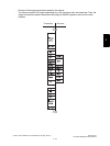
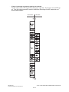
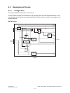
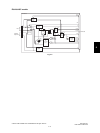
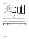
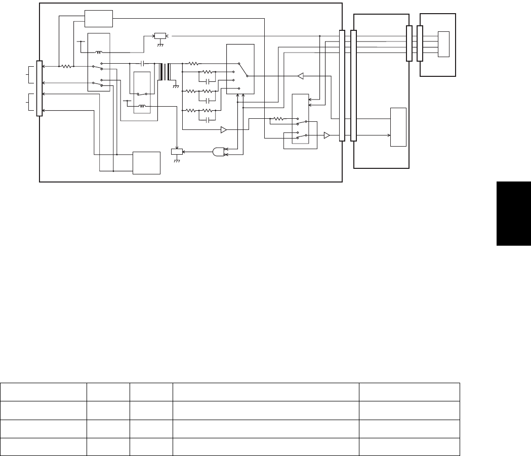
EU/AU/AS/C models
Fig. 4-5
The line path switching control circuit consists of the CML relay (RLY3) and analog switch (IC3, IC5) on
the NCU board, the ASIC (IC23) on the MAIN board, and the other peripheral devices. It changes the
path for the FAX send/receive signals and connects it to each control circuit.
The CML relay is switched according to the CML1 signal output from the ASIC on the MAIN board.
When the CML1 signal goes HIGH, Q4 comes on to turn ON the CML relay.
The analog switch (IC3) is switched according to the CML1 signal and ATT3DB1 signal. When the
CML1 signal or ATT3DB1 signal goes HIGH, the analog switch is turned ON.
The analog switch (IC5) is switched according to the RLADJ11 and RLADJ12 signals.
The analog switch is switched according to the states of the RLADJ11 and RLADJ21 signals.
Turning ON the CML relay and analog switch allow the MODEM to be connected to the line.
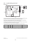
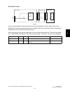
* Values in [ ] are GD-1221 in case that the descriptions vary between GD-1220 and GD-1221.
Signal Name Type Active Description Destination
CML1 O H Line 1 CML Relay Control Signal RLY3, IC3
ATT3DB1 O H Line 1 Attenuator Control Signal IC3
RLADJ11, 21 O H Line 1 Return Loss Adjustment Signal IC5
CN3
Lb
La
4
3
a2
b2
2
5
External
telephone
Line
0
1
10
8
0
1
3
3
1
2
4
5
121
4
9
+12V
RLY3
CML relay
T1
AG
NCU board
AG
Q4
13
11
3
10
14
15
16
5
4
7
12
1
2
Ring signal
detection
circuit
0
1
2
3
R28
R26
R29
R31
R32
IC5
Analog switch
C13
R36
C12
R30
C14
IC6
67
IC4
IC7
R11
1
2
13
12
14
15
10
11
0
1
0
1
IC3
Analog
switch
Line current
detection
circuit
CML1
ATT3DB1
RLADJ11
RLADJ21
TXOUT1
RXIN1
3
1
2
6
IC6
6
3
2
1
22
21
8
7
8
7
63
29
32
[
29
]
28,29
[
25,26
]
FAX board
CN4
CN262
AG
Q9
IC23
ASIC
IC12
[
IC2
]
MODEM
+12V
C7
RLY4
Relay
CN5
CN5
22
21
63
29
142
144
140
141
MAIN board
08/08