


ADSP-BF538F EZ-KIT Lite Evaluation System Manual I-3
INDEX
H
Help, online, xix
I
installation, of this EZ-KIT Lite, 1-5
interfaces, See audio, CAN, ELVIS, expansion,
SDRAM
internal memory
core/system MMRs, 1-8
data banks A, B SRAM, 1-8
data banks A, B SRAM/CACHE, 1-8
instruction banks A, B SRAM, 1-8
instruction SRAM/CACHE, 1-8
reserved, 1-8
scratch pad SRAM, 1-8
via JTAG, 2-9
internal regulator, 2-2
IO voltage, 2-2
J
JTAG
connector (ZP4), 2-23
emulation port, 2-9
jumpers
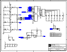
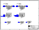
diagram of locations, 2-9
JP1 (PPI dir control), 2-13
JP6 (ELVIS voltage), 2-16
JP8 (ELVIS select), 2-16
JP9 (UART), 2-14
L
LabVIEW virtual instruments, xi, 1-12
LEDs
diagram of locations, 2-17
LED2-6 (PC5-9), 1-13, 2-19
LED7 (power), 2-18
LED8 (reset), 2-18
ZLED3 (USB monitor), 1-5, 2-19
LEFT_IN signal, 2-15
LEFT_OUT signal, 2-14
license restrictions,
x, 1-7
LOOPBACK signal, 2-10
M
Media Instruction Set Computing (MISC), ix
memory
map, of this EZ-KIT Lite, 1-7
select pins, See ~AMS3-0, ~SMS0
Micro Signal Architecture (MSA),
ix
MISO2 signal, 2-5
MOSI0-1 signals, 2-5
MOSI2 signal, 2-5
N
notation conventions, xxi
NU signal, 2-10, 2-13
O
oscilloscope configuration switch (SW1), 2-14
P
package contents, 1-3
PB1-4 (SW13-10) push buttons, 2-11
PCx signals, See programmable flags
PDx signals, See programmable flags
PEx signals, See programmable flags
PFx signals, See programmable flags
power
connector (J7), 2-22
LED (LED7), 2-18
supply, 1-3
PPI
connector (P8), 2-23
direction control (JP1) jumper, 2-13
PPI_CLK_SEL signal, 2-6
PPI_D4-15 signals, 2-7