


INDEX
I-4 ADSP-BF538F EZ-KIT Lite Evaluation System Manual
PPI_DIR_CTL signal, 2-6
PPI_FS3 signal, 2-7
programmable flags
PC0 (UART transmit), 1-11, 2-4, 2-10
PC1 (UART receive), 1-11, 2-4, 2-10
PC5-9 (LED2-6), 1-13, 2-19
PD0-8 signals, 2-5
PD10-13, 2-6
PD7 (JP1), 2-13
PD9 (ERR), 1-11, 2-6, 2-10
PE0-15, 2-6
PF0-3 (SW13-10), 1-13, 2-7, 2-11, 2-18
PF4-15 (PPI), 2-7
push buttons
See also switches by name (SWx)
diagram of locations, 2-17
R
real-time clock (RTC), 2-3
Reduced Instruction Set Computing (RISC),
ix
regulators, 2-2
reset
LEDs (LED8), 2-18
processor, 2-8
push button (SW9), 2-17
restriction, of the evaluation license, 1-7
RFS0 signal, 2-12
RFS2-3 signals, 2-6
RIGHT_IN signal, 2-15
RIGHT_OUT signal, 2-14
RS-232 connectors (J6),
xii, 2-21
RSCLK0 signal, 2-12
RSCLK2-3 signals, 2-6
RTS signal, 2-10
RX0 signal, 2-10
RX1-2 signals, 2-6
RXDx (receive data output) signals, 1-11, 2-10
S
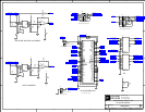
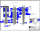
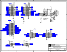
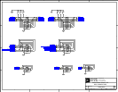
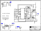
schematic, of ADSP-BF538F EZ-KIT Lite, B-1
SCLKx signals, 1-10, 2-5, 2-6
SDRAM
connections, 2-3
default settings, 1-9
interface, 1-8
memory map, 1-8
optimum settings, 1-9, 1-10
serial clock (SCL) signals, 1-9
serial peripheral interface, See SPI, SPI signals
~SMS0 (SDRAM select) pin, 1-7, 2-3
SPI
connector (P9), 2-24
interface, 2-4
SPI0SEL1-7 signals, 2-7
SPI1SEL signal, 2-5
SPI1SS signal, 2-5
SPI2SEL signal, 2-6
SPI2SS signal, 2-6
SPISS signal, 2-7
SPORT0
connector (P6), 2-23
interface, 1-12, 2-4, 2-8
SPORT1
connector (P7), 2-23
interface, 2-4, 2-8
SRAM, 1-7
See also internal memory
startup, of this EZ-KIT Lite, 1-5
STB (standby control input) signals, 2-10
stereo input/output channels, 1-12
SW10-13 (PD13-10) push buttons, 2-7, 2-18
SW14 (FCE enable) switch, 2-12
SW1 (audio/oscilloscope) switch, 2-14
SW2 (CAN enable) switch, 1-11, 2-10
SW3 (boot mode select) switch, 2-13
SW4 (UART) switch, 2-10
SW5 (push button enable) DIP switch, 1-13,
2-11, 2-18