


ADSST-SALEM-3T
Rev. 0 | Page 13 of 24
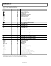
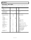
Parameter Min Typ Max Unit Test Conditions
FREQUENCY RESPONSE
(ADC)
7
Typical Output Frequency
(Normalized to f
S
)
0 0 dB
0.03125 –0.1 dB
0.0625 –0.25 dB
0.125 –0.6 dB
0.1875 –1.4 dB
0.25 –2.8 dB
0.3125 –4.5 dB
0.375 –7.0 dB
0.4375 –9.5 dB
> 0.5 < –12.5 dB
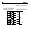
LOGIC INPUTS
V
INH
, Input High Voltage V
DD
– 0.8 V
DD
V
V
INL
, Input Low Voltage 0 0.8 V
I
IH
, Input Current 10
µA
C
IN
, Input Capacitance 10 pF
LOGIC OUTPUT
V
OH
, Output High Voltage V
DD
– 0.4 V
DD
V
|I
OUT
| ≤ 100 µA
V
OL
, Output Low Voltage 0 0.4 V
|I
OUT
| ≤ 100 µA
Three-State Leakage Current –10 +10
µA
POWER SUPPLIES
AVDD1, AVDD2 2.7 3.6 V
DVDD 2.7 3.6 V
IDD
8
See Table 7
1
Operating temperature range is as follows: –40°C to +85°C. Therefore, T
MIN
= –40°C and T
MAX
= +85°C.
2
Test conditions: Input PGA set for 0 dB gain (unless otherwise noted).
3
At input to sigma-delta modulator of ADC.
4
Guaranteed by design.
5
Overall group delay will be affected by the sample rate and the external digital filtering.
6
The ADC’s input impedance is inversely proportional to DMCLK and is approximated by: (4 × 10
11
)/DMCLK.
7
Frequency response of the ADC measured with input at audio reference level (the input level that produces an output level of 0 dBm0), with 38 dB preamplifier
bypassed and input gain of 0 dB.
8
Test Conditions: no load on digital inputs, analog inputs ac-coupled to ground.
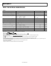
Table 7. Current Summary (AVDD = DVDD = 3.3 V)
Conditions
Digital Current,
Max (mA)
SE MCLK ON Comments
ADCs Only On 25 1 Yes REFOUT Disabled
REFCAP Only On 1.0 0 No REFOUT Disabled
REFCAP and REFOUT Only On 3.5 0 No
All Sections On 26.5 1 Yes REFOUT Enabled
All Sections Off 1.0 1 Yes MCLK Active Levels Equal to 0 V and DVDD
All Sections Off 0.05 0 No Digital Inputs Static and Equal to 0 V or DVDD
The above values are in mA and are typical values, unless otherwise noted. MCLK = 16.384 MHz; SCLK = 16.384 MHz.