


ADSST-SALEM-3T
Rev. 0 | Page 15 of 24
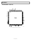
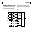
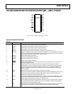
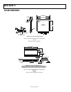
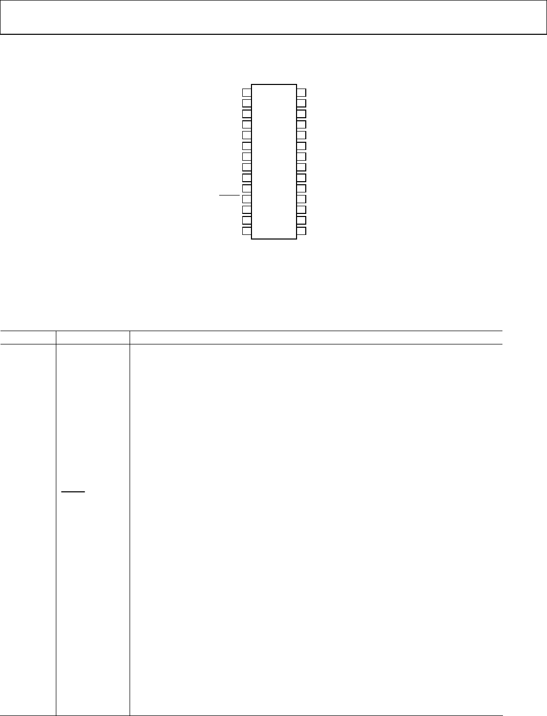
PIN CONFIGURATION AND PIN FUNCTION DESCRIPTIONS—ADSST-73360LAR
NC = NO CONNECT
TOP VIEW
(Not to Scale)
VINP2
1
VINN2
2
VINP1
3
VINN1
4
REFOUT
5
REFCAP
6
AVDD2
7
AGND2
8
DGND
9
DVDD
10
RESET
11
SCLK
12
MCLK
13
SDO
14
VINN3
VINP3
VINN4
VINP4
VINN5
28
24
27
26
25
VINP5
VINN6
VINP6
AVDD1
20
23
22
21
AGND1
SE
SDI
SDIFS
16
19
18
17
SDOFS
15
03738-0-005
Figure 7. ADSST-73360LAR Pin Configuration—RW-28
PIN FUNCTION DESCRIPTIONS
Table 9.
Pin No. Mnemonic Function
1 VINP2 Analog Input to the Positive Terminal of Input Channel 2.
2 VINN2 Analog Input to the Negative Terminal of Input Channel 2.
3 VINP1 Analog Input to the Positive Terminal of Input Channel 1.
4 VINN1 Analog Input to the Negative Terminal of Input Channel 1.
5 REFOUT Buffered Output of the Internal Reference, which has a nominal value of 1.2 V.
6 REFCAP
Reference Voltage for ADCs. A bypass capacitor to AGND2 of 0.1 µF is required for the on-chip
reference. The capacitor should be fixed to this pin. The internal reference can be overdriven
by an external reference connected to this pin if required.
7 AVDD2 Analog Power Supply Connection.
8 AGND2 Analog Ground/Substrate Connection.
9 DGND Digital Ground/Substrate Connection.
10 DVDD Digital Power Supply Connection.
11
RESET
Active Low Reset Signal. This input resets the entire chip, resetting the control registers and
clearing the digital circuitry.
12 SCLK
Output Serial Clock whose rate determines the serial transfer rate to/from the ADSST-
73360LAR. It is used to clock data or control information to and from the serial port (SPORT).
The frequency of SCLK is equal to the frequency of the master clock (MCLK) divided by an
integer number that is the product of the external master clock rate divider and the serial
clock rate divider.
13 MCLK Master Clock Input. MCLK is driven from an external clock signal.
14 SDO
Serial Data Output of the ADSST-73360LAR. Both data and control information may be output
on this pin and are clocked on the positive edge of SCLK. SDO is in three-state when no
information is being transmitted and when SE is low.
15 SDOFS
Framing Signal Output for SDO Serial Transfers. The frame sync is one bit wide and it is active
one SCLK period before the first bit (MSB) of each output word. SDOFS is referenced to the
positive edge of SCLK. SDOFS is in three-state when SE is low.
16 SDIFS
Framing Signal Input for SDI Serial Transfers. The frame sync is one bit wide and it is valid one
SCLK period before the first bit (MSB) of each input word. SDIFS is sampled on the negative
edge of SCLK and is ignored when SE is low.
17 SDI
Serial Data Input of the ADSST-73360LAR. Both data and control information may be input on
this pin and are clocked on the negative edge of SCLK. SDI is ignored when SE is low.