


ADSST-SALEM-3T
Rev. 0 | Page 17 of 24
POWER-UP INITIALIZATION AND DATA FROM THE
ADSST-SALEM-3T
The ADSST-SALEM-3T-EV boot loads the code from the
nonvolatile flash memory as shown in the block diagram of
a functional meter in Figure 1. The configuration and calibra-
tion data also gets loaded from the nonvolatile memory. For
further details on boot loading, refer to the ADSST-SALEM-3T-
DK (Developer’s Kit) User Manual. The user manual also
describes various commands for instantaneous and computed
parameters.
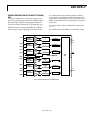
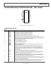
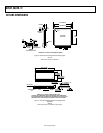
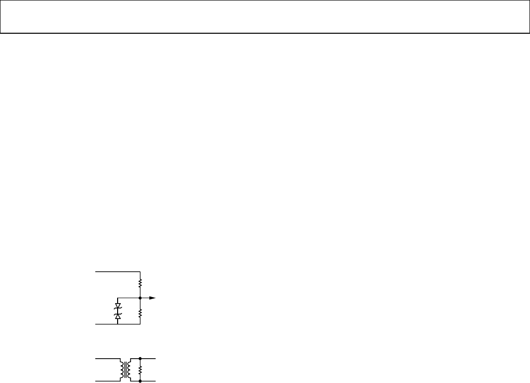
VOLTAGE AND CURRENT SENSING
Figure 9 shows the input section for the voltage and current
sections. Based on the voltage and current values, the GUI
software in the ADSST-SALEM-3T-DK computes the values of
resistors R1, R2, and R3. The closest available values to those
calculated by the GUI software should be selected and used.
R3
CURRENT INPUT
TO ADC
CHANNEL
NEUTRAL
PHASE
CURRENT
R2
VOLTAGE INPUT
TO ADC
CHANNEL
NEUTRAL
PHASE
VOLTAGE
R1
03738-0-007
Figure 9. Input Section
The ADSST-73360LAR has a peak-to-peak input range of V
REF
–
(V
REF
× 0.6525) to V
REF
+ (V
REF
× 0.6525); for V
REF
= 2.5 V, this is
0.856 V to 4.14 V p-p. This limit defines the resistance network
on the potential circuits and the burden resistance on the sec-
ondary side of the CT. Since the ADSST-73360LAR is a unipolar
ADC, the ac potential and current signals have to be offset by
some dc level. The reference design has a dc offset of 2.5 V. This
limits the peak-to-peak signal range of potential and current to
3.28 V p-p or 1.16 V rms.
Potential Section
The selection of the potential divider circuit should be such that
it can:
• Handle high surge voltages
• Have minimum VA burden
• Give approximately 1 V peak headroom to accommodate
overvoltages.
Current Section
The selection of CT ratio and burden resistance should be such
that it can:
• Handle the complete dynamic range for the current signal
input.
• Give approximately 1 V peak headroom to accommodate
loads with high crest factors.
The reference design has a CT with a turns ratio of 1:2500 and
burden resistance of 82 Ω. This generates 0.656 V rms or
0.928 V peak at 20 A current. This leaves enough margin for
current pulses or low crest factor loads, such as SMPS. The
maximum current can be up to 32.768 A.