


ADSST-SALEM-3T
Rev. 0 | Page 4 of 24
GENERAL DESCRIPTION OF THE ADSST-218X DSP
The ADSST-218x is a single-chip microcomputer optimized for
digital signal processing (DSP) and other high speed numeric
processing applications.
The DSP combines the ADSP-2100 family base architecture
(three computational units, data address generators, and a pro-
gram sequencer) with two serial ports, a 16-bit internal DMA
port, a byte DMA port, a programmable timer, flag I/O, exten-
sive interrupt capabilities, and on-chip program and data
memory.
The ADSST-218x is fabricated in a high speed, low power
CMOS process. Every instruction can execute in a single proc-
essor cycle.
The ADSST-218x’s flexible architecture and comprehensive
instruction set enable the processor to perform multiple opera-
tions in parallel. In one processor cycle, the ADSST-218x can:
• Generate the next program address
• Fetch the next instruction
• Perform one or two data moves
• Update one or two data address pointers
• Perform a computational operation
This takes place while the processor continues to:
• Receive and transmit data through the two serial ports
• Receive and/or transmit data through the internal
DMA port
• Receive and/or transmit data through the byte DMA port
• Decrement timer
ARCHITECTURE OVERVIEW
The ADSST-218x instruction set provides flexible data moves
and multifunction (one or two data moves with a computation)
instructions. Every instruction can be executed in a single proc-
essor cycle. The ADSST-218x assembly language uses an
algebraic syntax for ease of coding and readability. A compre-
hensive set of development tools supports program
development.
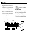
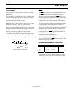
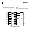
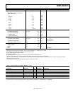
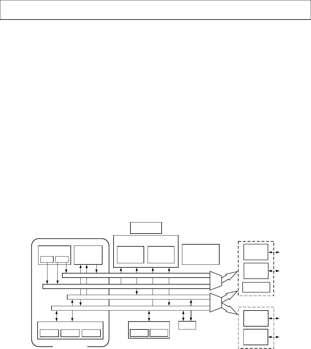
Figure 3 is the functional block diagram of the ADSST-218x.
The processor contains three independent computational units:
the ALU, the multiplier/accumulator (MAC), and the shifter.
The computational units process 16-bit data directly and have
provisions to support multiprecision computations.
OR
MEMORY
POWER-DOWN
CONTROL
DATA ADDRESS
GENERATORS
PROGRAM
SEQUENCER
ARITHMETIC UNITS SERIAL PORTS
DATA MEMORY DATA
TIMER
FULL MEMORY MODE
HOST MODE
EXTERNAL
ADDRESS
BUS
EXTERNAL
DATA
BUS
EXTERNAL
DATA
BUS
INTERNAL
DMA
PORT
BYTE DMA
CONTROLLER
SPORT0
DAG1 DAG2
ALU MAC SHIFTER
ADSP-2100 BASE
ARCHITECTURE
SPORT1
PROGRAM MEMORY ADDRESS
DATA MEMORY ADDRESS
PROGRAM MEMORY DATA
PROGRAM
MEMORY
16K × 24-BIT
DATA
MEMORY
16K × 16-BIT
PROGRAMMABLE
I/O
AND
FLAGS
03738-0-008
Figure 3. Functional Block Diagram