


ADSST-SALEM-3T
Rev. 0 | Page 7 of 24
CLOCK SIGNALS
Either a crystal or a TTL compatible clock signal can clock the
ADSST-218x.
If an external clock is used, it should be a TTL compatible signal
running at half the instruction rate. The signal is connected to
the processor’s CLKIN input. When an external clock is used,
the XTAL input must be left unconnected.
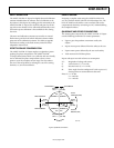
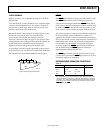
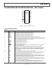
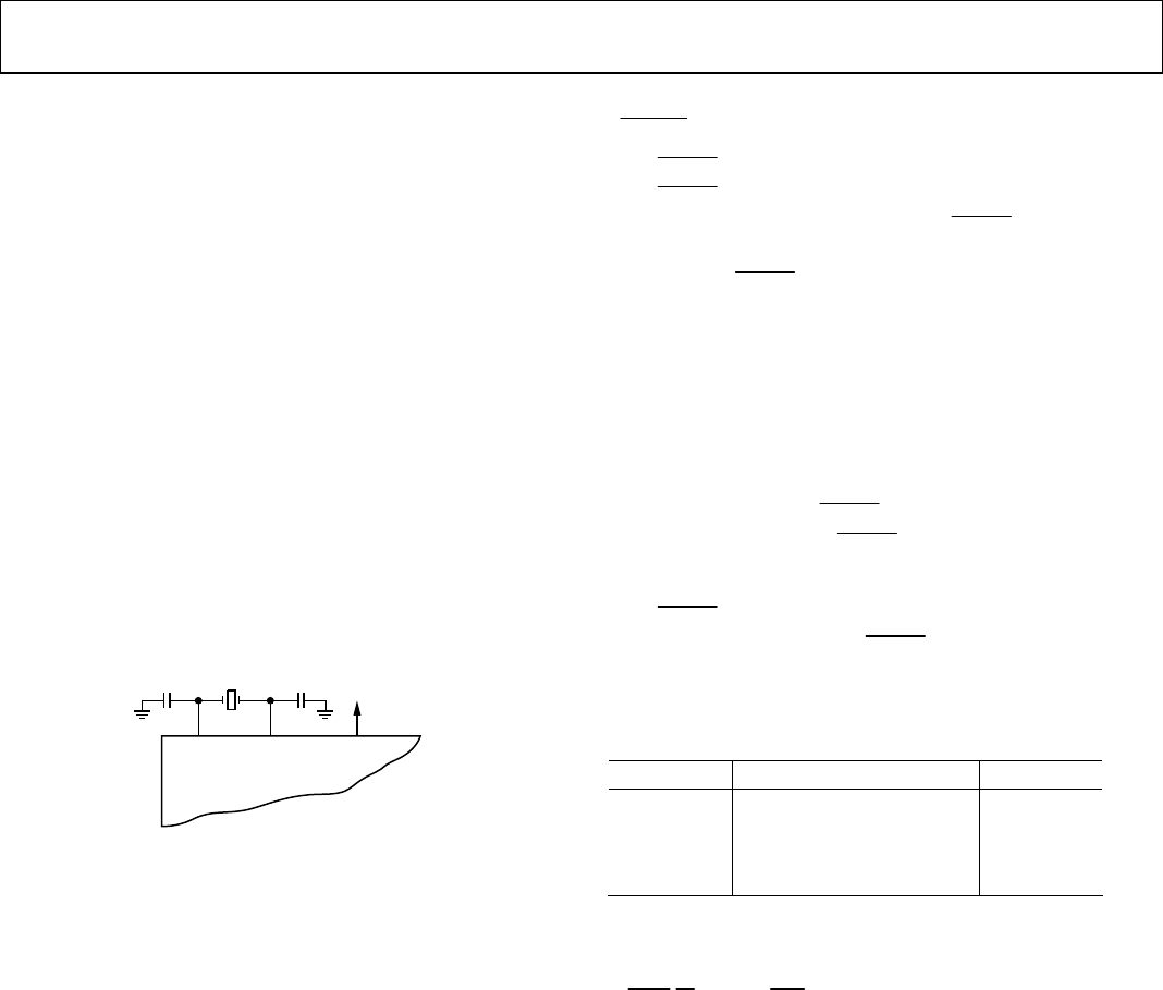
Because the ADSST-218x includes an on-chip oscillator circuit,
an external crystal may be used. The crystal should be
connected across the CLKIN and XTAL pins, with two
capacitors connected as shown in Figure 4. The capacitor values
are dependent on the crystal type and should be specified by the
crystal manufacturer. A parallel resonant, fundamental
frequency, microprocessor grade crystal should be used.
A clock output (CLKOUT) signal is generated by the processor
at the processor’s cycle rate. This can be enabled and disabled by
the CLKODIS bit in the SPORT0 autobuffer control register.
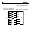
CLKIN XTAL
DSP
CLKOUT
03738-0-003
Figure 4. External Crystal Connections
RESET
The
RESET
signal initiates a master reset of the ADSST-2185x.
The
RESET
signal must be asserted during the power-up
sequence to assure proper initialization.
RESET
during initial
power-up must be held long enough to enable the internal clock
to stabilize. If
RESET
is activated any time after power-up, the
clock continues to run and does not require stabilization time.
The power-up sequence is defined as the total time required for
the crystal oscillator circuit to stabilize after a valid V
DD
is
applied to the processor and for the internal phase-locked loop
(PLL) to lock onto the specific crystal frequency. A minimum of
2000 CLKIN cycles ensures that the PLL has locked but does
not include the crystal oscillator start-up time. During this
power-up sequence, the
RESET
signal should be held low. On
any subsequent resets, the
RESET
signal must meet the
minimum pulse-width specification, t
RSP
.
The
RESET
input contains some hysteresis; however, if an RC
circuit is used to generate the
RESET
signal, the use of an exter-
nal Schmitt trigger is recommended.
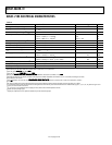
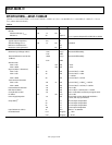
RECOMMENDED OPERATING CONDITIONS
Table 3.
Parameter Min Max Unit
V
DDINT
2.37 2.63 V
V
DDEXT
2.37 3.60 V
V
INPUT
1
V
IL
= –0.3 V
IH
= 3.6 V
T
AMB
0 70 °C
1
The ADSST-2185x is 3.3 V tolerant (always accepts up to 3.6 V max V
IH
), but
voltage compliance (on output, V
OH
) depends on the input V
DDEXT
; because
V
OH
(MAX) = V
DDEXT
(MAX). This applies to bidirectional pins (D0–D23, RFS0,
RFS1, SCLK0, SCLK1, TFS0, A1–A13, PF0–PF7) and input only pins (CLKIN,
RESET
,
BR
, DR0, DR1,
PWD
).