


REV. 0
Information furnished by Analog Devices is believed to be accurate and
reliable. However, no responsibility is assumed by Analog Devices for its
use, nor for any infringements of patents or other rights of third parties that
may result from its use. No license is granted by implication or otherwise
under any patent or patent rights of Analog Devices.
a
AD9883A
One Technology Way, P.O. Box 9106, Norwood, MA 02062-9106, U.S.A.
Tel: 781/329-4700 www.analog.com
Fax: 781/326-8703 © Analog Devices, Inc., 2001
110 MSPS/140 MSPS Analog Interface for
Flat Panel Displays
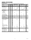
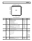
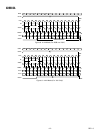
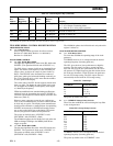
FUNCTIONAL BLOCK DIAGRAM
R
AIN
R
OUTA
G
AIN
G
OUTA
B
AIN
B
OUTA
MIDSCV
SYNC
PROCESSING
AND CLOCK
GENERATION
HSYNC
COAST
CLAMP
FILT
DTACK
HSOUT
VSOUT
SOGOUT
REF
REF
BYPASS
SERIAL REGISTER
AND
POWER MANAGEMENT
SCL
SDA
A
0
AD9883A
CLAMP
8
A/D
CLAMP
8
A/D
CLAMP
8
A/D
FEATURES
140 MSPS Maximum Conversion Rate
300 MHz Analog Bandwidth
0.5 V to 1.0 V Analog Input Range
500 ps p-p PLL Clock Jitter at 110 MSPS
3.3 V Power Supply
Full Sync Processing
Sync Detect for ”Hot Plugging”
Midscale Clamping
Power-Down Mode
Low Power: 500 mW Typical
4:2:2 Output Format Mode
APPLICATIONS
RGB Graphics Processing
LCD Monitors and Projectors
Plasma Display Panels
Scan Converters
Microdisplays
Digital TV
GENERAL DESCRIPTION
The AD9883A is a complete 8-bit, 140 MSPS monolithic analog
interface optimized for capturing RGB graphics signals from
personal computers and workstations. Its 140 MSPS encode
rate capability and full power analog bandwidth of 300 MHz
supports resolutions up to SXGA (1280 × 1024 at 75 Hz).
The AD9883A includes a 140 MHz triple ADC with internal
1.25 V reference, a PLL, and programmable gain, offset, and
clamp control. The user provides only a 3.3 V power supply,
analog input, and HSYNC and COAST signals. Three-state
CMOS outputs may be powered from 2.5 V to 3.3 V.
The AD9883A’s on-chip PLL generates a pixel clock from
HSYNC and COAST inputs. Pixel clock output frequencies
range from 12 MHz to 140 MHz. PLL clock jitter is 500 ps p-p
typical at 140 MSPS. When the COAST signal is presented,
the PLL maintains its output frequency in the absence of
HSYNC. A sampling phase adjustment is provided. Data,
HSYNC and Clock output phase relationships are maintained.
The AD9883A also offers full sync processing for composite
sync and sync-on-green applications.
A clamp signal is generated internally or may be provided by the
user through the CLAMP input pin. This interface is fully pro-
grammable via a 2-wire serial interface.
Fabricated in an advanced CMOS process, the AD9883A is
provided in a space-saving 80-lead LQFP surface mount plastic
package and is specified over the 0°C to 70°C temperature range.