


REV. 0
AD9883A
–21–
Data is read from the control registers of the AD9883A in a similar
manner. Reading requires two data transfer operations:
The base address must be written with the R/W bit of the slave
address byte LOW to set up a sequential read operation.
Reading (the R/W bit of the slave address byte high) begins at
the previously established base address. The address of the read
register autoincrements after each byte is transferred.
To terminate a read/write sequence to the AD9883A, a stop
signal must be sent. A stop signal comprises a low-to-high tran-
sition of SDA while SCL is high.
A repeated start signal occurs when the master device driving
the serial interface generates a start signal without first generat-
ing a stop signal to terminate the current communication. This
is used to change the mode of communication (read, write)
between the slave and master without releasing the serial inter-
face lines.
Serial Interface Read/Write Examples
Write to one control register
➥ Start Signal
➥ Slave Address Byte (R/W Bit = LOW)
➥ Base Address Byte
➥ Data Byte to Base Address
➥ Stop Signal
Write to four consecutive control registers
➥ Start Signal
➥ Slave Address Byte (R/W Bit = LOW)
➥ Base Address Byte
➥ Data Byte to Base Address
➥ Data Byte to (Base Address + 1)
➥ Data Byte to (Base Address + 2)
➥ Data Byte to (Base Address + 3)
➥ Stop Signal
Read from one control register
➥ Start Signal
➥ Slave Address Byte (R/W Bit = LOW)
➥ Base Address Byte
➥ Start Signal
➥ Slave Address byte (R/W bit = HIGH)
➥ Data Byte from Base Address
➥ Stop Signal
Read from four consecutive control registers
➥ Start Signal
➥ Slave Address Byte (R/W Bit = LOW)
➥ Base Address Byte
➥ Start Signal
➥ Slave Address Byte (R/W Bit = HIGH)
➥ Data Byte from Base Address
➥ Data Byte from (Base Address + 1)
➥ Data Byte from (Base Address + 2)
➥ Data Byte from (Base Address + 3)
➥ Stop Signal
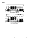
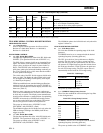
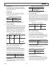
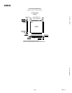
BIT 7
ACKBIT 6 BIT 5 BIT 4 BIT 3 BIT 2 BIT 1 BIT 0SDA
SCL
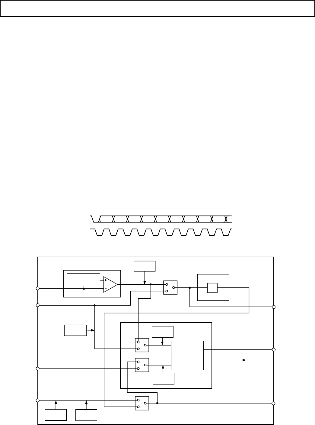
Figure 11. Serial Interface—Typical Byte Transfer
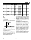
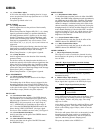
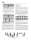
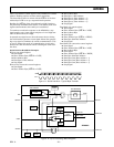
SYNC STRIPPER
ACTIVITY
DETECT
NEGATIVE PEAK
CLAMP
COMP
SYNC
SOG
HSYNC IN
ACTIVITY
DETECT
MUX 2
HSYNC OUT
PIXEL CLOCK
MUX 1
SYNC SEPARATOR
INTEGRATOR
VSYNC
SOG OUT
HSYNC OUT
VSYNC OUT
MUX 4
VSYNC IN
1/S
PLL
HSYNC
ACTIVITY
DETECT
AD9883A
CLOCK
GENERATOR
POLARITY
DETECT
POLARITY
DETECT
POLARITY
DETECT
MUX 3
COAST
COAST
Figure 12. Sync Processing Block Diagram