


REV. 0
AD9883A
–23–
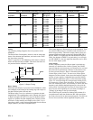
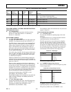
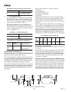
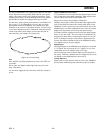
It is also recommended to use a single ground plane for the entire
board. Experience has repeatedly shown that the noise perfor-
mance is the same or better with a single ground plane. Using
multiple ground planes can be detrimental because each separate
ground plane is smaller, and long ground loops can result.
In some cases, using separate ground planes is unavoidable. For
those cases, it is recommended to at least place a single
ground plane under the AD9883A. The location of the split
should be at the receiver of the digital outputs. For this case it
is even more important to place components wisely because the
current loops will be much longer (current takes the path of
least resistance). An example of a current loop:
P
O
W
E
R
P
L
A
N
E
A
D
9
8
8
3
A
D
I
G
I
T
A
L
O
U
T
P
U
T
T
R
A
C
E
A
N
A
L
O
G
G
R
O
U
N
D
P
L
A
N
E
D
I
G
I
T
A
L
G
R
O
U
N
D
P
L
A
N
E
D
I
G
I
T
A
L
D
A
T
A
R
E
C
E
I
V
E
R
Figure 13. Current Loop
PLL
Place the PLL loop filter components as close to the FILT pin
as possible.
Do not place any digital or other high-frequency traces near
these components.
Use the values suggested in the data sheet with 10% tolerances
or less.
Outputs (Both Data and Clocks)
Try to minimize the trace length that the digital outputs have to
drive. Longer traces have higher capacitance, which requires more
current, which causes more internal digital noise.
Shorter traces reduce the possibility of reflections.
Adding a series resistor of value 50 Ω to 200 Ω can suppress reflec-
tions, reduce EMI, and reduce the current spikes inside of the
AD9883A. If series resistors are used, place them as close to the
AD9883A pins as possible (although try not to add vias or extra
length to the output trace in order to get the resistors closer).
If possible, limit the capacitance that each of the digital outputs
drives to less than 10pF. This can easily be accomplished by
keeping traces short and by connecting the outputs to only one
device. Loading the outputs with excessive capacitance will
increase the current transients inside of the AD9883A creating
more digital noise on its power supplies.
Digital Inputs
The digital inputs on the AD9883A were designed to work with
3.3 V signals, but are tolerant of 5.0 V signals. So, no extra
components need to be added if using 5.0 V logic.
Any noise that gets onto the Hsync input trace will add jitter to
the system. Therefore, minimize the trace length and do not run
any digital or other high-frequency traces near it.
Voltage Reference
Bypass with a 0.1 µF capacitor. Place as close to the AD9883A
pin as possible. Make the ground connection as short as possible.