


REV. 0
AD9883A
–17–
0E 5 Hsync Output Polarity
One bit that determines the polarity of the Hsync output
and the SOG output. Table XI shows the effect of this
option. SYNC indicates the logic state of the sync pulse.
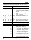
Table XI. Hsync Output Polarity Settings
Setting SYNC
0 Logic 1 (Positive Polarity)
1 Logic 0 (Negative Polarity)
The default setting for this register is 0.
0E 4 Active Hsync Override
This bit is used to override the automatic Hsync selection,
To override, set this bit to Logic 1. When overriding, the
active Hsync is set via Bit 3 in this register.
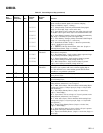
Table XII. Active Hsync Override Settings
Override Result
0 Auto Determines the Active Interface
1 Override, Bit 3 Determines the Active Interface
The default for this register is 0.
0E 3 Active Hsync Select
This bit is used under two conditions. It is used to select
the active Hsync when the override bit is set, (Bit 4). Alter-
nately, it is used to determine the active Hsync when not
overriding but both Hsyncs are detected.
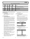
Table XIII. Active HSYNC Select Settings
Select Result
0 HSYNC Input
1 Sync-on-Green Input
The default for this register is 0.
0E 2 Vsync Output Invert
One bit that can invert the polarity of the Vsync output.
Table XIV shows the effect of this option.
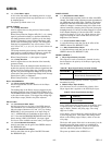
Table XIV. Vsync Output Invert Settings
Setting Vsync Output
1 No Invert
0 Invert
The default setting for this register is 1.
0E 1 Active Vsync Override
This bit is used to override the automatic Vsync selection.
To override, set this bit to Logic 1. When overriding, the
active interface is set via Bit 0 in this register.
Table XV. Active Vsync Override Settings
Override Result
0 Auto Determine the Active Vsync
1 Override, Bit 0 Determines the Active Vsync
The default for this register is 0.
0E 0 Active Vsync Select
This bit is used to select the active Vsync when the over-
ride bit is set (Bit 1).
Table XVI. Active Vsync Select Settings
Select Result
0 Vsync Input
1 Sync Separator Output
The default for this register is 0.
0F 7 Clamp Input Signal Source
A bit that determines the source of clamp timing.
Table XVII. Clamp Input Signal Source Settings
Clamp Function Function
0 Internally Generated Clamp
1 Externally Provided Clamp Signal
A 0 enables the clamp timing circuitry controlled by clamp
placement and clamp duration. The clamp position and
duration is counted from the leading edge of Hsync.
A 1 enables the external CLAMP input pin. The three
channels are clamped when the CLAMP signal is active.
The polarity of CLAMP is determined by the Clamp
Polarity bit (Register 0Fh, Bit 6).
The power-up default value is Clamp Function = 0.
0F 6 Clamp Input Signal Polarity
A bit that determines the polarity of the externally pro-
vided CLAMP signal.
Table XVIII. Clamp Input Signal Polarity Settings
Clamp Function Function
1 Active LOW
0 Active HIGH
A Logic 1 means that the circuit will clamp when CLAMP is
HIGH, and it will pass the signal to the ADC when CLAMP
is LOW.
A Logic 0 means that the circuit will clamp when CLAMP
is LOW, and it will pass the signal to the ADC when
CLAMP is HIGH.
The power-up default value is Clamp Polarity = 1.
0F 5 Coast Select
This bit is used to select the active coast source. The
choices are the coast input pin or Vsync. If Vsync is selected
the additional decision of using the Vsync input pin or the
output from the sync separator needs to be made (Reg-
ister 0E, Bits 1, 0).
Table XIX. Power-Down Settings
Select Result
0 Coast Input Pin
1 Vsync (See above Text)