


REV. 0
AD9883A
–8–
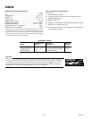
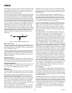
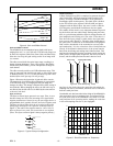
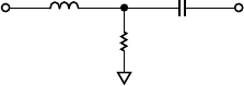
At that point the signal should be resistively terminated (75 Ω
to the signal ground return) and capacitively coupled to the
AD9883A inputs through 47 nF capacitors. These capacitors
form part of the dc restoration circuit.
In an ideal world of perfectly matched impedances, the best perfor-
mance can be obtained with the widest possible signal bandwidth.
The ultrawide bandwidth inputs of the AD9883A (300 MHz)
can track the input signal continuously as it moves from one pixel
level to the next, and digitize the pixel during a long, flat pixel
time. In many systems, however, there are mismatches, reflections,
and noise, which can result in excessive ringing and distortion of
the input waveform. This makes it more difficult to establish a
sampling phase that provides good image quality. It has been
shown that a small inductor in series with the input is effec-
tive in rolling off the input bandwidth slightly, and providing
a high quality signal over a wider range of conditions. Using a
Fair-Rite #2508051217Z0 High-Speed Signal Chip Bead
inductor in the circuit of Figure 1 gives good results in most
applications.
RGB
INPUT
R
AIN
G
AIN
B
AIN
47nF
75⍀
Figure 1. Analog Input Interface Circuit
Hsync, Vsync Inputs
The interface also takes a horizontal sync signal, which is used
to generate the pixel clock and clamp timing. This can be either
a sync signal directly from the graphics source, or a preprocessed
TTL or CMOS level signal.
The Hsync input includes a Schmitt trigger buffer for immunity
to noise and signals with long rise times. In typical PC-based
graphic systems, the sync signals are simply TTL-level drivers
feeding unshielded wires in the monitor cable. As such, no ter-
mination is required.
Serial Control Port
The serial control port is designed for 3.3 V logic. If there are 5 V
drivers on the bus, these pins should be protected with 150 Ω series
resistors placed between the pull-up resistors and the input pins.
Output Signal Handling
The digital outputs are designed and specified to operate from a
3.3 V power supply (V
DD
). They can also work with a V
DD
as
low as 2.5 V for compatibility with other 2.5 V logic.
Clamping
RGB Clamping
To properly digitize the incoming signal, the dc offset of the input
must be adjusted to fit the range of the on-board A/D converters.
Most graphics systems produce RGB signals with black at
ground and white at approximately 0.75 V. However, if sync
signals are embedded in the graphics, the sync tip is often at
ground and black is at 300 mV. Then white is at approximately
1.0 V. Some common RGB line amplifier boxes use emitter-
follower buffers to split signals and increase drive capability.
This introduces a 700 mV dc offset to the signal, which must be
removed for proper capture by the AD9883A.
The key to clamping is to identify a portion (time) of the signal
when the graphic system is known to be producing black. An
offset is then introduced which results in the A/D converters
producing a black output (code 00h) when the known black
input is present. The offset then remains in place when other
signal levels are processed, and the entire signal is shifted to elimi-
nate offset errors.
In most PC graphics systems, black is transmitted between
active video lines. With CRT displays, when the electron beam
has completed writing a horizontal line on the screen (at the
right side), the beam is deflected quickly to the left side of the
screen (called horizontal retrace) and a black signal is provided
to prevent the beam from disturbing the image.
In systems with embedded sync, a blacker-than-black signal
(Hsync) is produced briefly to signal the CRT that it is time to
begin a retrace. For obvious reasons, it is important to avoid
clamping on the tip of Hsync. Fortunately, there is virtually
always a period following Hsync called the back porch where a
good black reference is provided. This is the time when clamp-
ing should be done.
The clamp timing can be established by simply exercising the
CLAMP pin at the appropriate time (with External Clamp = 1).
The polarity of this signal is set by the Clamp Polarity bit.
A simpler method of clamp timing employs the AD9883A internal
clamp timing generator. The Clamp Placement register is pro-
grammed with the number of pixel times that should pass after
the trailing edge of HSYNC before clamping starts. A second
register (Clamp Duration) sets the duration of the clamp.
These are both 8-bit values, providing considerable flexibility in
clamp generation. The clamp timing is referenced to the trailing
edge of Hsync because, though Hsync duration can vary widely,
the back porch (black reference) always follows Hsync. A good
starting point for establishing clamping is to set the clamp place-
ment to 09h (providing 9 pixel periods for the graphics signal to
stabilize after sync) and set the clamp duration to 14h (giving
the clamp 20 pixel periods to reestablish the black reference).
Clamping is accomplished by placing an appropriate charge on
the external input coupling capacitor. The value of this capaci-
tor affects the performance of the clamp. If it is too small, there
will be a significant amplitude change during a horizontal line
time (between clamping intervals). If the capacitor is too large,
then it will take excessively long for the clamp to recover from a
large change in incoming signal offset. The recommended value
(47 nF) results in recovering from a step error of 100 mV to
within 1/2 LSB in 10 lines with a clamp duration of 20 pixel
periods on a 60 Hz SXGA signal.
YUV Clamping
YUV graphic signals are slightly different from RGB signals in
that the dc reference level (black level in RGB signals) can be at
the midpoint of the graphics signal rather than the bottom. For
these signals it can be necessary to clamp to the midscale range
of the A/D converter range (80h) rather than bottom of the A/D
converter range (00h).
Clamping to midscale rather than ground can be accomplished
by setting the clamp select bits in the serial bus register. Each of
the three converters has its own selection bit so that they can be
clamped to either midscale or ground independently. These bits
are located in register 10h and are Bits 0–2. The midscale refer-
ence voltage that each A/D converter clamps to is provided on
the MIDSCV pin, (Pin 37). This pin should be bypassed to
ground with a 0.1 µF capacitor, (even if midscale clamping is
not required).