


REV. 0
AD9883A
–7–
PIN FUNCTION DESCRIPTIONS (continued)
Pin Name Function
CLAMP External Clamp Input
This logic input may be used to define the time during which the input signal is clamped to ground. It should be
exercised when the reference dc level is known to be present on the analog input channels, typically during the back
porch of the graphics signal. The CLAMP pin is enabled by setting control bit Clamp Function to 1, (register 0FH,
Bit 7, default is 0). When disabled, this pin is ignored and the clamp timing is determined internally by counting a
delay and duration from the trailing edge of the HSYNC input. The logic sense of this pin is controlled by Clamp
Polarity register 0FH, Bit 6. When not used, this pin must be grounded and Clamp Function programmed to 0.
COAST Clock Generator Coast Input (Optional)
This input may be used to cause the pixel clock generator to stop synchronizing with Hsync and continue producing a
clock at its current frequency and phase. This is useful when processing signals from sources that fail to produce
horizontal sync pulses during the vertical interval. The COAST signal is generally not required for PC-generated
signals. The logic sense of this pin is controlled by Coast Polarity (register 0FH, Bit 3). When not used, this pin
may be grounded and Coast Polarity programmed to 1, or tied HIGH (to V
D
through a 10 kΩ resistor) and Coast
Polarity programmed to 0. Coast Polarity defaults to 1 at power-up.
REF BYPASS Internal Reference BYPASS
Bypass for the internal 1.25 V bandgap reference. It should be connected to ground through a 0.1 µF capacitor.
The absolute accuracy of this reference is ±4%, and the temperature coefficient is ±50 ppm, which is adequate for
most AD9883A applications. If higher accuracy is required, an external reference may be employed instead.
MIDSCV Midscale Voltage Reference BYPASS
Bypass for the internal midscale voltage reference. It should be connected to ground through a 0.1 µF capacitor.
The exact voltage varies with the gain setting of the Blue channel.
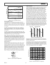
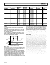
FILT External Filter Connection
For proper operation, the pixel clock generator PLL requires an external filter. Connect the filter shown in Figure 6
to this pin. For optimal performance, minimize noise and parasitics on this node.
POWER SUPPLY
V
D
Main Power Supply
These pins supply power to the main elements of the circuit. They should be as quiet and filtered as possible.
V
DD
Digital Output Power Supply
A large number of output pins (up to 25) switching at high speed (up to 110 MHz) generates a lot of power supply
transients (noise). These supply pins are identified separately from the V
D
pins so special care can be taken to minimize
output noise transferred into the sensitive analog circuitry. If the AD9883A is interfacing with lower voltage logic,
V
DD
may be connected to a lower supply voltage (as low as 2.5 V) for compatibility.
PV
D
Clock Generator Power Supply
The most sensitive portion of the AD9883A is the clock generation circuitry. These pins provide power to the clock PLL
and help the user design for optimal performance. The designer should provide “quiet,” noise-free power to these pins.
GND Ground
The ground return for all circuitry on chip. It is recommended that the AD9883A be assembled on a single solid
ground plane, with careful attention to ground current paths.
DESIGN GUIDE
General Description
The AD9883A is a fully integrated solution for capturing analog
RGB signals and digitizing them for display on flat panel monitors
or projectors. The circuit is ideal for providing a computer interface
for HDTV monitors or as the front end to high-performance video
scan converters.
Implemented in a high-performance CMOS process, the interface
can capture signals with pixel rates of up to 110 MHz.
The AD9883A includes all necessary input buffering, signal dc
restoration (clamping), offset and gain (brightness and contrast)
adjustment, pixel clock generation, sampling phase control, and
output data formatting. All controls are programmable via a 2-wire
serial interface. Full integration of these sensitive analog functions
makes system design straightforward and less sensitive to the
physical and electrical environment.
With a typical power dissipation of only 500 mW and an operating
temperature range of 0°C to 70°C, the device requires no special
environmental considerations.
Digital Inputs
All digital inputs on the AD9883A operate to 3.3 V CMOS levels.
However, all digital inputs are 5 V tolerant. (Applying 5 V to
them will not cause any damage.)
Input Signal Handling
The AD9883A has three high-impedance analog input pins
for the Red, Green, and Blue channels. They will accommodate
signals ranging from 0.5 V to 1.0 V p-p.
Signals are typically brought onto the interface board via a
DVI-I connector, a 15-pin D connector, or via BNC connectors.
The AD9883A should be located as close as practical to the input
connector. Signals should be routed via matched-impedance
traces (normally 75 Ω) to the IC input pins.