


REV. 0
AD9883A
–10–
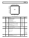
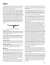
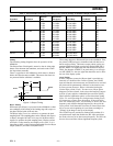
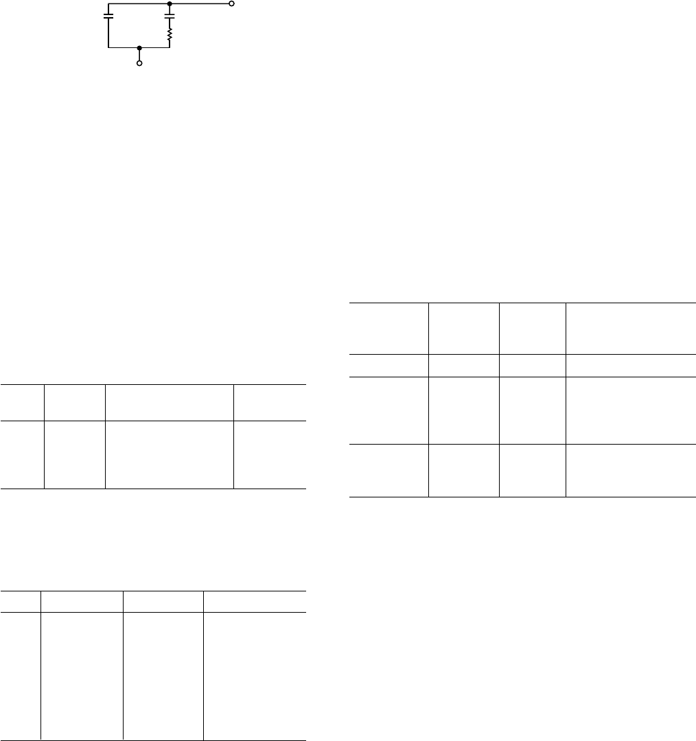
The PLL characteristics are determined by the loop filter design,
by the PLL Charge Pump Current and by the VCO range setting.
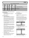
The loop filter design is illustrated in Figure 6. Recommended
settings of VCO range and charge pump current for VESA
standard display modes are listed in Table V.
C
P
0.0039F
0.039F C
Z
3.3k⍀ R
Z
FILT
PV
D
Figure 6. PLL Loop Filter Detail
Four programmable registers are provided to optimize the per-
formance of the PLL. These registers are:
1. The 12-Bit Divisor Register. The input Hsync frequencies
range from 15 kHz to 110 kHz. The PLL multiplies the
frequency of the Hsync signal, producing pixel clock
frequencies in the range of 12 MHz to 110 MHz. The
Divisor Register controls the exact multiplication factor.
This register may be set to any value between 221 and 4095.
(The divide ratio that is actually used is the programmed
divide ratio plus one.)
2. The 2-Bit VCO Range Register. To improve the noise
performance of the AD9883A, the VCO operating frequency
range is divided into three overlapping regions. The VCO
Range Register sets this operating range. The frequency
ranges for the lowest and highest regions are shown in Table II.
Table II. VCO Frequency Ranges
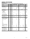
Pixel Clock Range K
VCO
Gain
PV1 PV0 (MHz) (MHz/V)
0 0 12–36 150
0 1 36–72 150
1 0 72–110 150
1 1 110-140 150
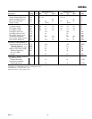
3. The 3-Bit Charge Pump Current register. This register
allows the current that drives the low pass loop filter to be
varied. The possible current values are listed in Table III.
Table III. Charge Pump Current/Control Bits
Ip2 Ip1 Ip0 Current (A)
00 0 50
0 0 1 100
0 1 0 150
0 1 1 250
1 0 0 350
1 0 1 500
1 1 0 750
1 1 1 1500
4. The 5-Bit Phase Adjust Register. The phase of the generated
sampling clock may be shifted to locate an optimum sampling
point within a clock cycle. The Phase Adjust register provides
32 phase-shift steps of 11.25° each. The Hsync signal with
an identical phase shift is available through the HSOUT pin.
The COAST pin is used to allow the PLL to continue to run
at the same frequency, in the absence of the incoming HSYNC
signal or during disturbances in Hsync (such as equalization
pulses). This may be used during the vertical sync period, or
any other time that the HSYNC signal is unavailable. The
polarity of the COAST signal may be set through the Coast
Polarity Register. Also, the polarity of the HSYNC signal
may be set through the HSYNC Polarity Register. For both
HSYNC and COAST, a value of “1” is active high.
Power Management
The AD9883A uses the activity detect circuits, the active inter-
face bits in the serial bus, the active interface override bits, and
the power-down bit to determine the correct power state. There
are three power states, full-power, seek mode, and power-down.
Table IV summarizes how the AD9883A determines what power
mode to be in and what circuitry is powered on/off in each of
these modes. The power-down command has priority and then
the automatic circuitry.
Table IV. Power-Down Mode Descriptions
Inputs
Power- Sync Powered On or
Mode Down
1
Detect
2
Comments
Full-Power 1 1 Everything
Seek Mode 1 0 Serial Bus, Sync
Activity Detect,
SOG,
Bandgap Reference
Power-Down 0 X Serial Bus, Sync
Activity Detect, SOG,
Bandgap Reference
NOTES
1
Power-Down is controlled via Bit 1 in serial bus register 0Fh.
2
Sync Detect is determined by OR-ing Bits 7, 4, and 1 in serial bus register 14h.