


ASUS A7V266-EX User’s Manual60
4. BIOS SETUP
4. BIOS SETUP
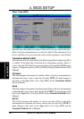
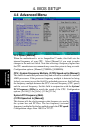
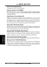
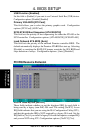
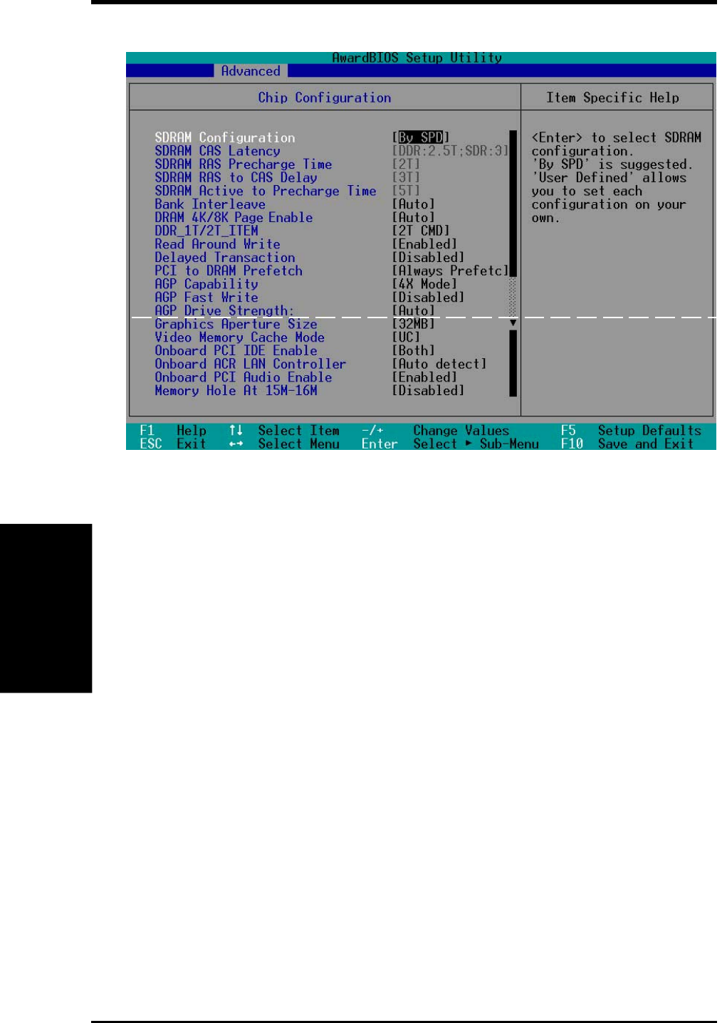
Chip Configuration
SDRAM Configuration [By SPD]
This sets the optimal timings for items 2–5, depending on the memory
modules that you are using. The default setting is [By SPD], which configures
items 2–5 by reading the contents in the SPD (Serial Presence Detect) device.
The EEPROM on the memory module stores critical parameter information
about the module, such as memory type, size, speed, voltage interface, and
module banks. Configuration options: [User Defined] [7ns (143MHz)] [8ns
(125MHz)] [By SPD]
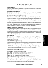
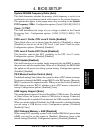
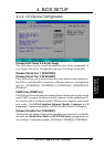
SDRAM CAS Latency [DDR:2.ST;SDR:3]
This controls the latency between the SDRAM read command and the
time that the data actually becomes available. NOTE: This field appears
only when you set the SDRAM Configuration to [User Defined].
Configuration options: [DDR:2.ST;SDR:3T] [2T]
SDRAM RAS Precharge Time [2T]
This controls the idle clocks after issuing a precharge command to the
SDRAM. NOTE: This field appears only when you set the SDRAM
Configuration to [User Defined]. Configuration options: [3T] [2T]
SDRAM RAS to CAS Delay [3T]
This controls the latency between the SDRAM active command and the
read/write command. NOTE: This field appears only if the SDRAM
Configuration is set: [User Defined]. Configuration options: [3T] [2T]
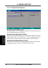
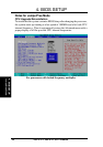
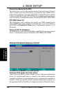
4.4.1 Chip Configuration
(Scroll down to see more items as shown)