


ASUS P5VD2-MX/P5V-VM DHASUS P5VD2-MX/P5V-VM DH
ASUS P5VD2-MX/P5V-VM DHASUS P5VD2-MX/P5V-VM DH
ASUS P5VD2-MX/P5V-VM DH
2-212-21
2-212-21
2-21
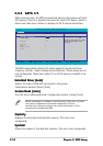
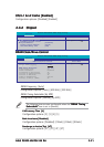
CPU L1 & L2 Cache [Enabled]CPU L1 & L2 Cache [Enabled]
CPU L1 & L2 Cache [Enabled]CPU L1 & L2 Cache [Enabled]
CPU L1 & L2 Cache [Enabled]
Configuration options: [Disabled] [Enabled]
Select Menu
Item Specific Help
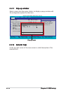
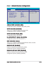
Phoenix-Award BIOS CMOS Setup Utility
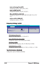
Advanced
Chipset
DRAM Clock/Drive Control
Frequency/Voltage control
Top Performance [Disabled]
Primary Display Adapter [PCI-E]
VGA Share Memory Size [64M]
2.4.22.4.2
2.4.22.4.2
2.4.2
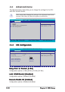
ChipsetChipset
ChipsetChipset
Chipset
DRAM Clock/Drive ControlDRAM Clock/Drive Control
DRAM Clock/Drive ControlDRAM Clock/Drive Control
DRAM Clock/Drive Control
Select Menu
Item Specific Help
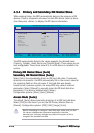
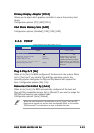
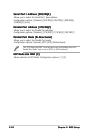
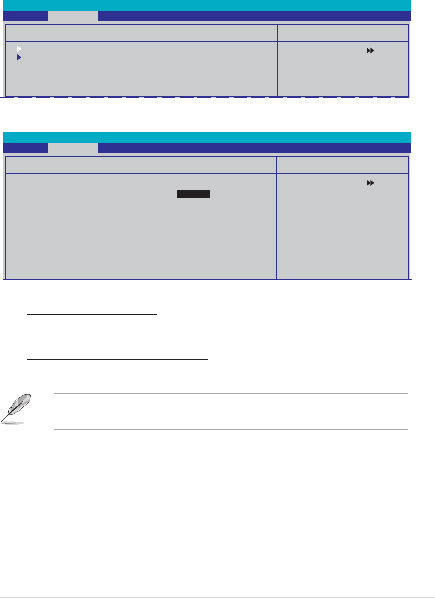
Phoenix-Award BIOS CMOS Setup Utility
Advanced
DRAM Clock/Drive Control
Current DRAM Frequency 200MHz
DRAM Frequency
DRAM Timing Selectable [By SPD]
x CAS Latency Time 4
x Bank Interleave Disabled
x Precharge to Active(Trp) 4T
x Active to Precharge(Tras) 07T
x Active to CMD(Trcd) 4T
x REF to ACT/REF(Trfc) 20T/21T
x ACT(0) to ACT(1) (TRRD) 3T
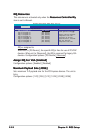
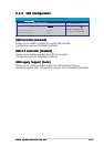
Auto
DRAM Frequency [Auto]
Configuration options: [Auto] [400 MHz] [533 MHz]
DRAM Timing Selectable [By SPD]
Configuration options: [Manual] [By SPD]
The following items are user-configurable when the
“DRAM Timing “DRAM Timing
“DRAM Timing “DRAM Timing
“DRAM Timing
Selectable”Selectable”
Selectable”Selectable”
Selectable” item is set to [Manual].
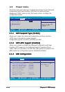
CAS Latency Time [4]CAS Latency Time [4]
CAS Latency Time [4]CAS Latency Time [4]
CAS Latency Time [4]
Configuration options: [2] [3] [4] [5]
Bank Interleave [Disabled]Bank Interleave [Disabled]
Bank Interleave [Disabled]Bank Interleave [Disabled]
Bank Interleave [Disabled]
Configuration options: [Disabled] [2 Bank] [4 Bank] [8 Bank]
Precharge to Active(Trp) [4T]Precharge to Active(Trp) [4T]
Precharge to Active(Trp) [4T]Precharge to Active(Trp) [4T]
Precharge to Active(Trp) [4T]
Configuration options: [2T] [3T] [4T] [5T]