


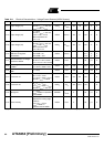
66
4929B–AUTO–01/07
ATA6264 [Preliminary]
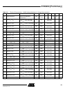
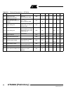
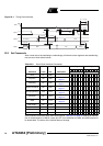
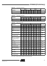
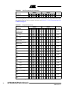
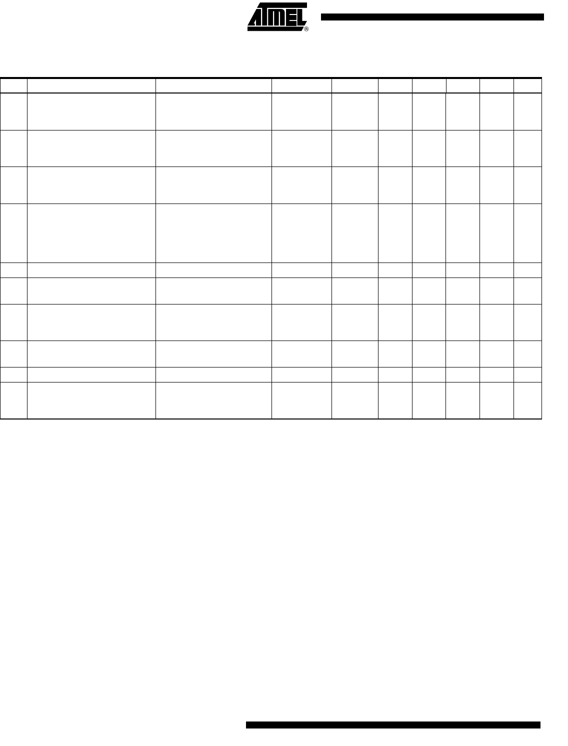
Table 20-1. Electrical Characteristics – UZP Buffer
No. Parameters Test Conditions Pin Symbol Min Typ. Max. Unit Type*
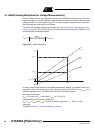
19.1
Output current high side,
driving current with
measurement activated
V
UZP
= 0V,
UZP connected to GND
UZP I
UZP
–8 –2 mA A
19.2
Output current low side,
sink current with measurement
activated
V
UZP
= V
VPERI
UZP connected to GND
UZP I
UZP
28mAA
19.3 Output settling time
Measured from rising edge
of SSQ to 90% of V
UZP
, no
load at pin UZP
UZP t
UZP
10 µs A
19.4 Output settling time
Load 2 kΩ/22 nF low-pass
filter connected to pin UZP,
measured from rising edge
of SSQ to 90% of
V
Low pass filter out
UZP t
UZP
250 µs A
19.5 Output resistance UZP R
UZP
100 Ω A
19.6 Linear measurement range UZP V
UZP
0.2
V
VPERI
– 0.2
VA
19.7 Maximum output voltage
V
IASG5
switched via AMUX
to UZP, V
IASG5
= 6V
UZP V
UZP
V
VPERI
–
50 mV
V
VPERI
+
50 mV
VA
19.8 Output leakage current
V
UZP
= 0V to V
VPERI
, UZP
buffer in tristate mode
UZP I
UZP
–5 +5 µA A
19.9 Output capacitance UZP buffer in tristate mode UZP C
UZP
010pFD
19.10 Time to switch to tristate mode
Measured from rising edge
of SSQ to I
leak
within
tolerance
UZP t
UZP
3µsA
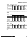
*) Type means: A = 100% tested, B = 100% correlation tested, C = Characterized on samples, D = Design parameter