


8
4929B–AUTO–01/07
ATA6264 [Preliminary]
4. Functional Range
Within the functional range, the ATA6264 works as specified. All voltages are referenced to the
ideal ground level of an ECU connected to the GNDA, GNDB and GNDD pins.
At the beginning of each specification table, supply voltage and temperature conditions are
described.
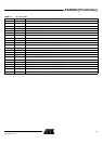
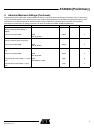
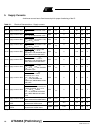
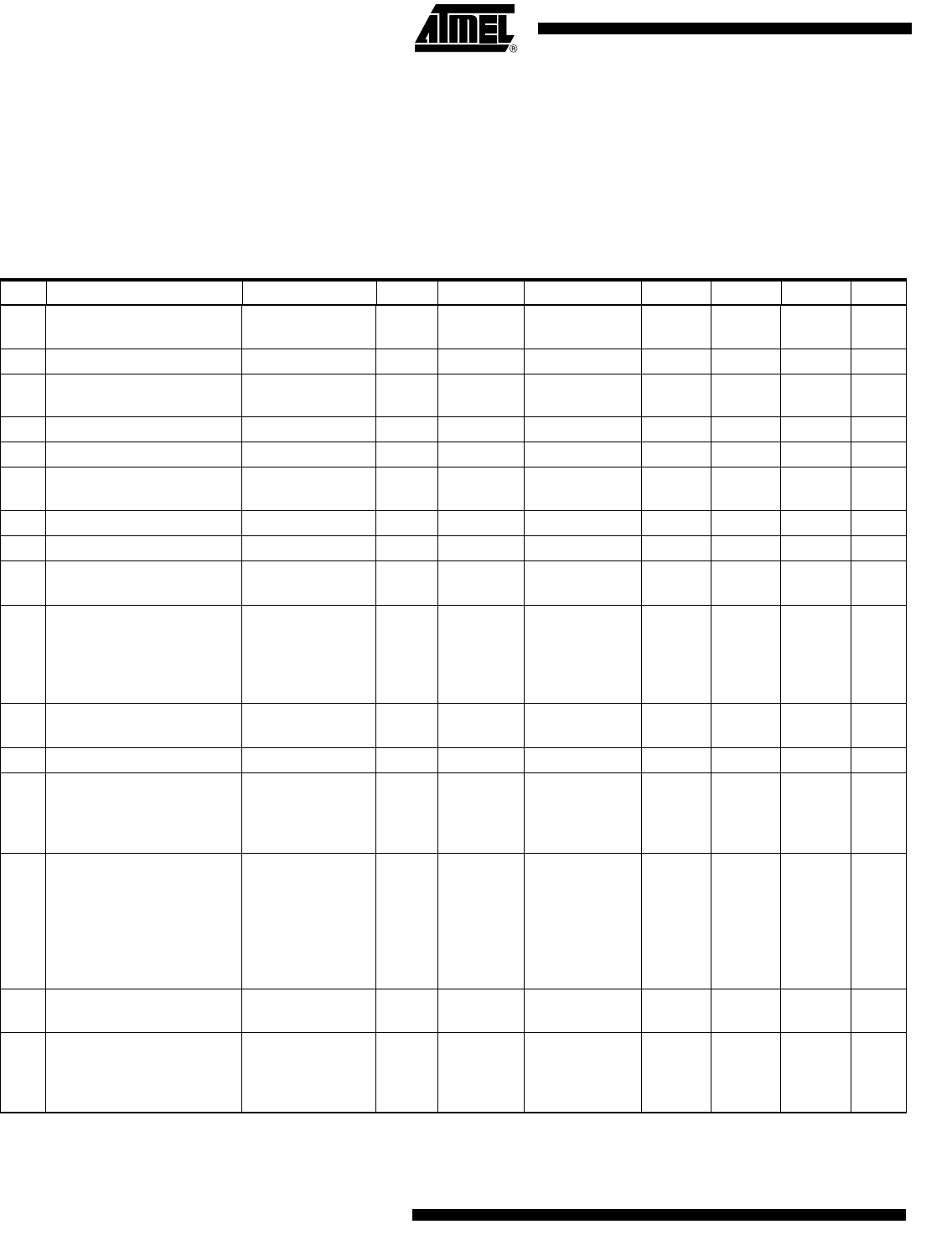
Table 4-1. Electrical Characteristics – Functional Range
No. Parameters Test Conditions Pin Symbol Min. Typ. Max. Unit Type*
1.1
Voltage on pins K30, K15,
USP
–0.3 +40 V
1.1a Voltage on pins K1, K2 –25 +40 V
1.2
Rate of supply voltage rise
(K30, K15, K1, K2)
50 V/µs
1.3 Supply voltage EVZ –0.3 +40 V
1.4 Supply voltage VSAT –0.3 +14 V
1.5
Supply voltages VCORE,
VPERI
–0.3 +5.5 V
1.6 Supply voltage CP, CP-OUT –0.3 +50 V
1.7 Voltage on digital I/O pins –0.3 +5.5 V
1.8
Voltage on pins SVSAT,
SVCORE
–1.0 +40 V
1.9
Voltage on pins UZP,
ISENS, COMCOI,
COMCOO, COMSATO,
COMSATI, COMEVZO,
FBEVZ, IREF, VINT
–0.3 +5.5 V
1.10
Voltage on pins GEVZ,
OCEVZ
–0.3 +10 V
1.11 Voltage on pin SVPERI –0.3 +6 V
1.12
Voltage on pins IASGx
(x = 1 to 5)
Voltage
necessary to
drive –40 mA
stored in 20 µH
40 V
1.14
Temperatures:
Operating ambient
temperature range
Operating junction
temperature range
Storage ambient/junction
temperature range
– 40
– 40
– 55
+ 90
+150
+105
°C
°C
°C
1.15
Thermal resistance junction
ambient
60 K/W
1.16
Substrate current which can
be drawn without
disturbances to upper
defined blocks/functions
(1)
–40 mA
*) Type means: A = 100% tested, B = 100% correlation tested, C = Characterized on samples, D = Design parameter
Note: 1. No substrate current occurs at pins K1, K2 down to V
K1
, V
K2
> –25V