


Rev. 2.01
- 39 -
SRP-350/352plusA&C
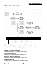
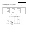
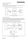
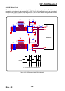
4-3-8 DIP Switch Circuit
The key board circuit consist of the scan signal of 3 lines and the return signal of 2-line. The CPU sends
repeatedly and continuously the scan data DIP_A~DIP. The DIP S/W information input in the return signal if
the specific DIP S/W is ON status during the given time. The CPU reads the data through DIP IN1~IN2 and
analyzes what DIP S/W is ON and performs the selected function.
CPU
uPD70F3107
+3.3V
R63 100F
RA10
10K 1/16W
1
2
3
4 5
6
7
8
RA9
10K 1/16W
1
2
3
4 5
6
7
8
0
RA12
10K 1/16W
1
2
3
4 5
6
7
8
DIP_B
0
SW2
218-008LPS
1 2
3 4
5 6
7 8
1615
1413
1211
109
R64 100F
0
0
SW1
218-008LPS
1 2
3 4
5 6
7 8
1615
1413
1211
109
DIP_IN1
RA11
10K 1/16W
1
2
3
4 5
6
7
8
DIP_C
0
BP48
100nF
DIP_IN2
+3.3V +3.3V
U15
74HC151/SOIC
4
3
2
1
15
14
13
12
11
10
9
7
16
8
5
6
D0
D1
D2
D3
D4
D5
D6
D7
A
B
C
STROBE
VCC
GND
Y
W
0
0
BP47
100nF
DIP_A
U14
74HC151/SOIC
4
3
2
1
15
14
13
12
11
10
9
7
16
8
5
6
D0
D1
D2
D3
D4
D5
D6
D7
A
B
C
STROBE
VCC
GND
Y
W
+3.3V
R62 100F
0
DIP_A
DIP_B
DIP_C
DIP1 DIP2 DIP3 DIP4 DIP5 DIP6 DIP7 DIP8
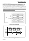
[Figure 4-12 USB Communication Block Diagram]