


DIGITAL-LOGIC AG MSB900/L Detailed Technical Manual V1.0
46
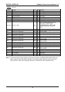
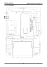
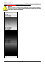
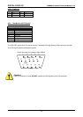
X15 Reverse Pin Configuration MSB900 LVDS X15 (on component side)
Attention!
When X15 is soldered on the component side, a different pin numbering schema must be applied.
Odd and even pin numbers are swapped. Ignoring this warning may result in the destruction
of any attached devices such as displays!
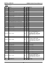
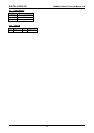
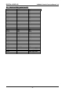
Pin Signal
1 VCC (+5V Output)
2 GND
3 LVDS_YAP0
4 LVDS_YAM0
5 VCC (+5V Output)
6 GND
7 LVDS_YAP1
8 LVDS_YAM1
9 VCC (+5V Output)
10 GND
11 LVDS_YAP2
12 LVDS_YAM2
13 Enable VDD
14 GND
15 LVDS_CLKAM
16 LVDS_CLKAP
17 CRT green
18 CRT red
19 CRT hsync
20 CRT blue
21 CRT SCL
22 CRT vsync
23 GND
24 CRT SDA
25 COM2 DSR
26 COM2 DCD
27 COM2 RTS
28 COM2 RXD
29 COM2 CTS
30 COM2 TXD
31 COM2 RI
32 COM2 DTR
33 VCC3 (+3.3V Output)
34 SYS_RST#
35 USB D+
36 USB D-
37 SMB SCL
38 VCC3 (+3.3V Output)
39 AVR PA0
40 SMB SDA
41 DCMAIN (filtered power input)
42 AVR PA3
43 VCC (+5V Output)
44 GND