


DIGITAL-LOGIC AG MSB900/L Detailed Technical Manual V1.0
51
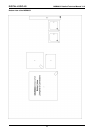
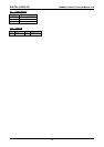
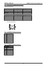
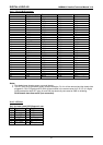
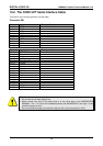
X101 PCI-104 BUS Interface
Pin A B C D
1 GND/5.0V KEY2 Reserved +5 AD00
2 VI/O AD02 AD01 +5V
3 AD05 GND AD04 AD03
4 C/BE0* AD07 GND AD06
5 GND AD09 AD08 GND
6 AD11 VI/O AD10 M66EN
7 AD14 AD13 GND AD12
8 +3.3V C/BE1* AD15 +3.3V
9 SERR* GND SB0* PAR
10 GND PERR* +3.3V SDONE
11 STOP* +3.3V LOCK* GND
12 +3.3V TRDY* GND DEVSEL*
13 FRAME* GND IRDY* +3.3V
14 GND AD16 +3.3V C/BE2*
15 AD18 +3.3V AD17 GND
16 AD21 AD20 GND AD19
17 +3.3V AD23 AD22 +3.3V
18 IDSEL0 GND IDSEL1 IDSEL2
19 AD24 C/BE3* VI/O IDSEL3
20 GND AD26 AD25 GND
21 AD29 +5V AD28 AD27
22 +5V AD30 GND AD31
23 REQ0* GND REQ1* VI/O
24 GND REQ2* +5V GNT0*
25 GNT1* VI/O GNT2* GND
26 +5V CLK0 GND CLK1
27 CLK2 +5V CLK3 GND
28 GND INTD* +5V RST*
29 +12V INTA* INTB* INTC*
30 -12V Reserved Reserved GND/3.3V KEY2
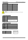
Notes:
1. The shaded area denotes power or ground signals.
2. The KEY pins are to guarantee proper module installation. Pin-A1 will be removed and the female side
plugged for 5.0V I/O signals and Pin-D30 will be modified in the same manner for 3.3V I/O. It is highly
recommended that both KEY pins (A1 and D30) be electrically connected to GND for shielding.
DLAG boards have them as NC (not connected).
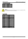
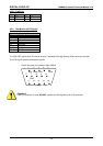
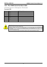
X110 LPC-Port
Only for factory and POD-Diagnostic use.
Pin Signal Pin Signal
1 VCC 3.3V 2 LAD0
3 LFrame# 4 LAD1
5 PCI_RST# 6 LAD2
7 FWH_TBL# 8 LAD3
9 VCC 5V 10 PCI_RST#
11 LPC_Clock 12 nc
13 Ground 14 FWH_Control