


DIGITAL-LOGIC AG MSEBX800/900 Detailed Manual V1.0
49
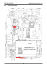
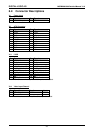
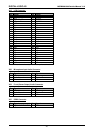
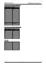
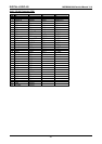
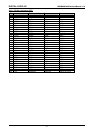
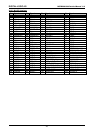
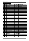
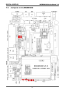
X130 PCI Slot (Standard PCI Slot)
Pin Name PCI Pin Description Pin Name PCI Pin Description
A1 TRST Test Logic Reset B1 -12V -12 VDC
A2 +12V +12 VDC B2 TCK Test Clock
A3 TMS Test Mde Select B3 GND Ground
A4 TDI Test Data Input B4 TDO Test Data Output
A5 +5V +5 VDC B5 +5V +5 VDC
A6 INTA Interrupt A B6 +5V +5 VDC
A7 INTC Interrupt C B7 INTB Interrupt B
A8 +5V +5 VDC B8 INTD Interrupt D
A9 ----- Reserved B9 PRSNT1 Present
A10 +5V Power (+5 V or +3.3 V) B10 ----- Reserved
A11 ----- Reserved B11 PRSNT2 Present
A12 GND03
Ground or Keyway for 3.3/Universal PWB
B12 GND
Ground or Keyway for 3.3/Universal PWB
A13 GND05
Ground or Keyway for 3.3/Universal PWB
B13 GND
Ground or Open (Key) for 3.3/Universal PWB
A14 3.3Vaux ----- B14 RES Reserved
A15 RESET Reset B15 GND Ground
A16 +5V Power (+5 V or +3.3 V) B16 CLK Clock
A17 GNT Grant PCI use B17 GND Ground
A18 GND08 Ground B18 REQ Request
A19 PME# Power Managment Event B19 +5V Power (+5 V or +3.3 V)
A20 AD30 Address/Data 30 B20 AD31 Address/Data 31
A21 +3.3V01 +3.3 VDC B21 AD29 Address/Data 29
A22 AD28 Address/Data 28 B22 GND Ground
A23 AD26 Address/Data 26 B23 AD27 Address/Data 27
A24 GND10 Ground B24 AD25 Address/Data 25
A25 AD24 Address/Data 24 B25 +3.3V +3.3VDC
A26 IDSEL Initialization Device Select B26 C/BE3 Command, Byte Enable 3
A27 +3.3V03 +3.3 VDC B27 AD23 Address/Data 23
A28 AD22 Address/Data 22 B28 GND Ground
A29 AD20 Address/Data 20 B29 AD21 Address/Data 21
A30 GND12 Ground B30 AD19 Address/Data 19
A31 AD18 Address/Data 18 B31 +3.3V +3.3 VDC
A32 AD16 Address/Data 16 B32 AD17 Address/Data 17
A33 +3.3V05 +3.3 VDC B33 C/BE2 Command, Byte Enable 2
A34 FRAME Address or Data phase B34 GND13 Ground
A35 GND14 Ground B35 IRDY# Initiator Ready
A36 TRDY# Target Ready B36 +3.3V06 +3.3 VDC
A37 GND15 Ground B37 DEVSEL Device Select
A38 STOP Stop Transfer Cycle B38 GND16 Ground
A39 +3.3V07 +3.3 VDC B39 LOCK# Lock bus
A40 ----- Reserved B40 PERR# Parity Error
A41 ----- Reserved B41 +3.3V08 +3.3 VDC
A42 GND17 Ground B42 SERR# System Error
A43 PAR Parity B43 +3.3V09 +3.3 VDC
A44 AD15 Address/Data 15 B44 C/BE1 Command, Byte Enable 1
A45 +3.3V10 +3.3 VDC B45 AD14 Address/Data 14
A46 AD13 Address/Data 13 B46 GND18 Ground
A47 AD11 Address/Data 11 B47 AD12 Address/Data 12
A48 GND19 Ground B48 AD10 Address/Data 10
A49 AD9 Address/Data 9 B49 GND20 Ground
A50 Keyway Open or Ground for 3.3V PWB B50 Keyway Open or Ground for 3.3V PWB
A51 Keyway Open or Ground for 3.3V PWB B51 Keyway Open or Ground for 3.3V PWB
A52 C/BE0 Command, Byte Enable 0 B52 AD8 Address/Data 8
A53 +3.3V11 +3.3 VDC B53 AD7 Address/Data 7
A54 AD6 Address/Data 6 B54 +3.3V12 +3.3 VDC
A55 AD4 Address/Data 4 B55 AD5 Address/Data 5
A56 GND21 Ground B56 AD3 Address/Data 3
A57 AD2 Address/Data 2 B57 GND22 Ground
A58 AD0 Address/Data 0 B58 AD1 Address/Data 1
A59 +5V Power (+5 V or +3.3 V) B59 VCC08 Power (+5 V or +3.3 V)
A60 REQ64 Request 64 bit B60 ACK64 Acknowledge 64 bit
A61 VCC11 +5 VDC B61 VCC10 +5 VDC
A62 VCC13 +5 VDC B62 VCC12 +5 VDC