


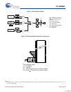

CY14B256K
Document Number: 001-06431 Rev. *H Page 14 of 28
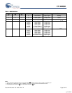
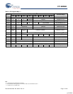
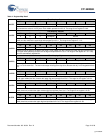
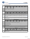
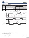
0x7FF4
Alarm - Hours
D7 D6 D5 D4 D3 D2 D1 D0
M 10s Alarm Hours Alarm Hours
Contains the alarm value for the hours and the mask bit to select or deselect the hours value.
M Match. When this bit is set to 0, the hours value is used in the alarm match. Setting this bit to 1 causes the match circuit
to ignore the hours value.
0x7FF3
Alarm - Minutes
D7 D6 D5 D4 D3 D2 D1 D0
M 10s Alarm Minutes Alarm Minutes
Contains the alarm value for the minutes and the mask bit to select or deselect the minutes value.
M Match. When this bit is set to 0, the minutes value is used in the alarm match. Setting this bit to 1 causes the match
circuit to ignore the minutes value.
0x7FF2
Alarm - Seconds
D7 D6 D5 D4 D3 D2 D1 D0
M 10s Alarm Seconds Alarm Seconds
Contains the alarm value for the seconds and the mask bit to select or deselect the seconds’ value.
M Match. When this bit is set to 0, the seconds value is used in the alarm match. Setting this bit to 1 causes the match
circuit to ignore the seconds value.
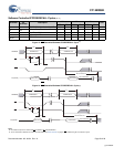
0x7FF1
Time Keeping - Centuries
D7 D6 D5 D4 D3 D2 D1 D0
10s Centuries Centuries
Contains the BCD value of centuries. Lower nibble contains the lower digit and operates from 0 to 9; upper nibble contains
the upper digit and operates from 0 to 9. The range for the register is 0-99 centuries.
0x7FF0
Flags
D7 D6 D5 D4 D3 D2 D1 D0
WDF AF PF OSCF 0 CAL W R
WDF Watchdog Timer Flag. This read only bit is set to 1 when the watchdog timer is allowed to reach 0 without being reset
by the user. It is cleared to 0 when the Flags register is read or on power-up.
AF Alarm Flag. This read only bit is set to 1 when the time and date match the values stored in the alarm registers with the
match bits = 0. It is cleared when the Flags register is read or on power-up.
PF Power Fail Flag. This read only bit is set to 1 when power falls below the power fail threshold V
SWITCH
. It is cleared to
0 when the Flags register is read or on power-up.
OSCF Oscillator Fail Flag. Set to 1 on power up if the oscillator is enabled and not running in the first 5 ms of operation. This
indicates that RTC backup power failed and clock value is no longer valid. The user must reset this bit to 0 to clear this
condition (Flag). The chip does not clear this flag. This bit survives power cycles.
CAL Calibration Mode. When set to 1, a 512 Hz square wave is output on the INT pin. When set to 0, the INT pin resumes
normal operation. This bit defaults to 0 (disabled) on power up.
W Write Enable: Setting the W bit to 1 freezes updatesof the RTC registers. The user can then write to RTC registers, Alarm
registers, Calibration register, Interrupt register and Flags register. Setting the W bit to 0 causes the contents of the RTC
registers to be transferred to the time keeping counters if the time has been changed (a new base time is loaded). This
bit defaults to 0 on power up.
R Read Enable: Setting R bit to 1, stops clock updates to user RTC registers so that clock updates are not seen during
the reading process. Set R bit to 0 to resume clock updates to the holding register. Setting this bit does not require W
bit to be set to 1. This bit defaults to 0 on power up.
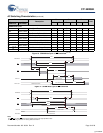
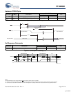
Table 4. Register Map Detail (continued)
[+] Feedback