


CY14B256K
Document Number: 001-06431 Rev. *H Page 17 of 28
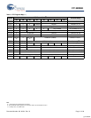
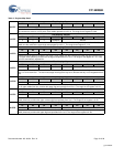
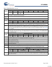
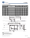
AC Switching Characteristics
Parameter
Description
25 ns 35 ns 45 ns
Unit
Min Max Min Max Min Max
Cypress
Parameter
Alt.
Parameter
SRAM Read Cycle
t
ACE
t
ELQV
Chip Enable Access Time 25 35 45 ns
t
RC
[10]
t
AVAV,
t
ELEH
Read Cycle Time 25 35 45 ns
t
AA
[11]
t
AVQV
Address Access Time 25 35 45 ns
t
DOE
t
GLQV
Output Enable to Data Valid 12 15 20 ns
t
OHA
[11]
t
AXQX
Output Hold After Address Change 3 3 3 ns
t
LZCE
[12]
t
ELQX
Chip Enable to Output Active 3 3 3 ns
t
HZCE
[12]
t
EHQZ
Chip Disable to Output Inactive 10 13 15 ns
t
LZOE
[12]
t
GLQX
Output Enable to Output Active 0 0 0 ns
t
HZOE
[12]
t
GHQZ
Output Disable to Output Inactive 10 13 15 ns
t
PU
[13]
t
ELICCH
Chip Enable to Power Active 0 0 0 ns
t
PD
[13]
t
EHICCL
Chip Disable to Power Standby 25 35 45 ns
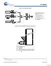
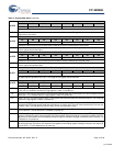
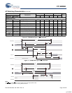
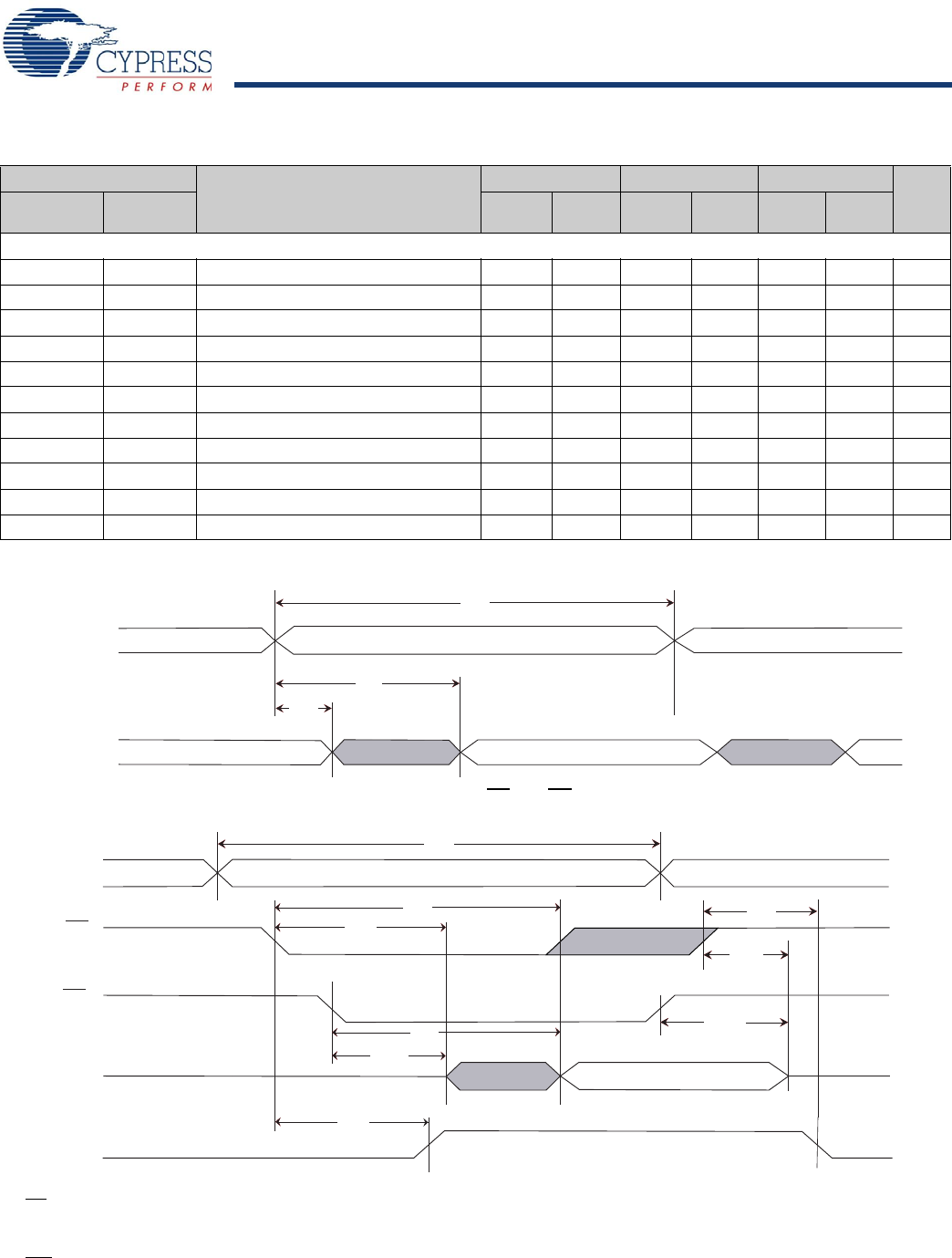
Figure 8. SRAM Read Cycle 1: Address Controlled
[10, 11, 14]
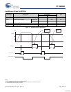
Figure 9. SRAM Read Cycle 2: CE and OE Controlled
[10, 14]
W
5&
W
$$
W
2+$
$''5(66
'4'$7$287
'$7$9$/,'
$''5(66
W
5&
&(
W
$&(
W
/=&(
W
3'
W
+=&(
2(
W
'2(
W
/=2(
W
+=2(
'$7$9$/,'
$&7,9(
67$1'%<
W
38
'4'$7$287
,&&
Notes
10.WE
is HIGH during SRAM Read Cycles.
11. Device is continuously selected with CE and OE both Low.
12.Measured ±200 mV from steady state output voltage.
13.These parameters are guaranteed by design and are not tested.
14.HSB
must remain HIGH during READ and WRITE cycles.
[+] Feedback