


CY14B256K
Document Number: 001-06431 Rev. *H Page 5 of 28
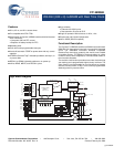
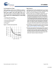
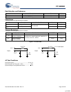
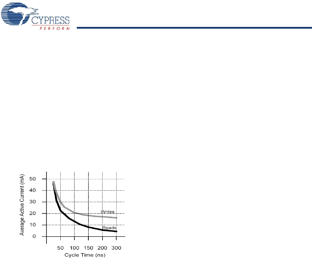
Low Average Active Power
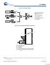
CMOS technology provides the CY14B256K the benefit of
drawing significantly less current when it is cycled at times longer
than 50 ns. Figure 3 shows the relationship between I
CC
and
READ and/or WRITE cycle time. Worst case current
consumption is shown for commercial temperature range, V
CC
=
3.6V, and chip enable at maximum frequency. Only standby
current is drawn when the chip is disabled. The overall average
current drawn by the CY14B256K depends on the following
items:
1. 1The duty cycle of chip enable
2. The overall cycle rate for accesses
3. The ratio of READs to WRITEs
4. The operating temperature
5. The V
CC
level
6. IO loading
Best Practices
nvSRAM products have been used effectively for over 15 years.
While ease-of-use is one of the product’s main system values,
experience gained working with hundreds of applications has
resulted in the following suggestions as best practices:
■ The nonvolatile cells in an nvSRAM are programmed on the
test floor during final test and quality assurance. Incoming
inspection routines at customer or contract manufacturer’s
sites sometimes reprograms these values. Final NV patterns
are typically repeating patterns of AA, 55, 00, FF, A5, or 5A.
The end product’s firmware should not assume that an NV array
is in a set programmed state. Routines that check memory
content values to determine first time system configuration and
cold or warm boot status must always program a unique NV
pattern (for example, complex 4-byte pattern of 46 E6 49 53
hex or more random bytes) as part of the final system manufac-
turing test to ensure these system routines work consistently.
■ The OSCEN bit in the Calibration register at 0x7FF8 should be
set to 1 to preserve battery life when the system is in storage
(see Stopping and Starting the Oscillator on page 7).
■ The Vcap value specified in this data sheet includes a minimum
and a maximum value size. The best practice is to meet this
requirement and not exceed the maximum Vcap value because
the higher inrush currents may reduce the reliability of the
internal pass transistor. Customers who want to use a larger
Vcap value to make sure there is extra store charge should
discuss their Vcap size selection with Cypress.
Figure 3. Current versus Cycle Time
[+] Feedback