


CY14B256K
Document Number: 001-06431 Rev. *H Page 9 of 28
Power Monitor
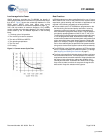
The CY14B256K provides a power management scheme with
power fail interrupt capability. It also controls the internal switch
to backup power for the clock and protects the memory from low
V
CC
access. The power monitor is based on an internal band gap
reference circuit that compares the V
CC
voltage to V
SWITCH
threshold.
As described in the “AutoStore® Operation” on page 3, when
V
SWITCH
is reached as V
CC
decays from power loss, a data store
operation is initiated from SRAM to the nonvolatile elements,
securing the last SRAM data state. Power is also switched from
V
CC
to the backup supply (battery or capacitor) to operate the
RTC oscillator.
When operating from the backup source, read and write opera-
tions to nvSRAM are inhibited and the clock functions are not
available to the user. The clock continues to operate in the
background. The updated clock data is available to the user
t
HRECALL
delay after V
CC
is restored to the device (see
“AutoStore or Power Up RECALL” on page 19).
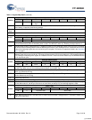
Interrupts
The CY14B256K has a Flags register, Interrupt register and
Interrupt logic that can signal interrupt to the microcontroller.
There are three potential sources for interrupt: watchdog timer,
power monitor, and alarm timer. Each of these can be individually
enabled to drive the INT pin by appropriate setting in the Interrupt
register (0x7FF6). In addition, each has an associated flag bit in
the Flags register (0x7FF0) that the host processor uses to
determine the cause of the interrupt. The INT pin driver has two
bits that specify its behavior when an interrupt occurs.
An Interrupt is raised only if both a flag is raised by one of the
three sources and the respective interrupt enable bit in Interrupts
register is enabled (set to ‘1’). After an interrupt source is active,
two programmable bits, H/L and P/L, determine the behavior of
the output pin driver on INT pin. These two bits are located in the
Interrupt register and can be used to drive level or pulse mode
output from the INT pin. In pulse mode, the pulse width is
internally fixed at approximately 200 ms. This mode is intended
to reset a host microcontroller. In the level mode, the pin goes to
its active polarity until the Flags register is read by the user. This
mode is used as an interrupt to a host microcontroller. The
control bits are summarized in the following section.
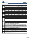
Interrupt Register
Watchdog Interrupt Enable - WIE. When set to ‘1’, the
watchdog timer drives the INT pin and an internal flag when a
watchdog time out occurs. When WIE is set to ‘0’, the watchdog
timer only affects the WDF flag in Flags register.
Alarm Interrupt Enable - AIE. When set to ‘1’, the alarm match
drives the INT pin and an internal flag. When AIE is set to ‘0’, the
alarm match only affects the AF flagin Flags register.
Power Fail Interrupt Enable - PFE. When set to ‘1’, the power
fail monitor drives the pin and an internal flag. When PFE is set
to ‘0’, the power fail monitor only affects the PF flag in Flags
register.
High/Low - H/L. When set to a ‘1’, the INT pin is active HIGH
and the driver mode is push pull. The INT pin drives high only
when V
CC
is greater than V
SWITCH
. When set to a ‘0’, the INT pin
is active LOW and the drive mode is open drain. Active LOW
(open drain) is operational even in battery backup mode.
Pulse/Level - P/L. When set to a ‘1’ and an interrupt occurs, the
INT pin is driven for approximately 200 ms. When P/L is set to a
‘0’, the INT pin is driven high or low (determined by H/L) until the
Flags or Control register is read.
When an enabled interrupt source activates the INT pin, an
external host reads the Flags registers to determine the cause.
Remember that all flags are cleared when the register is read. If
the INT pin is programmed for Level mode, then the condition
clears and the INT pin returns to its inactive state. If the pin is
programmed for Pulse mode, then reading the flag also clears
the flag and the pin. The pulse does not complete its specified
duration if the Flags register is read. If the INT pin is used as a
host reset, then the Flags or Control register is not read during a
reset.
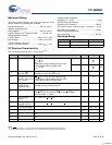
Flags Register
The Flag register has three flag bits: WDF, AF, and PF, which can
be used to generate an interrupt. These flags are set by the
watchdog timeout, alarm match, or power fail monitor respec-
tively. The processor can either poll this register or enable inter-
rupts to be informed when a flag is set. These flags are automat-
ically reset once the register is read. The flags register is
automatically loaded with the value 00h on power up (except for
the OSCF bit. See “Stopping and Starting the Oscillator” on
page 7.)
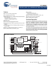
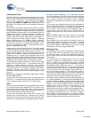
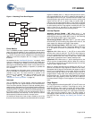
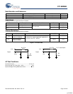
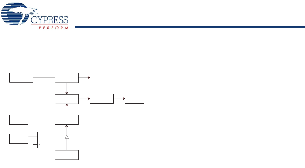
Figure 4. Watchdog Timer Block Diagram
1 Hz
Oscillator
Clock
Divider
Counter
Zero
Compare
WDF
WDS
Load
Register
WDW
D
Q
Q
Watchdog
Register
write to
Watchdog
Register
32 Hz
32,768 KHz
[+] Feedback