


CY14B256K
Document Number: 001-06431 Rev. *H Page 3 of 28
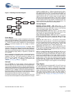
Device Operation
The CY14B256K nvSRAM consists of two functional
components paired in the same physical cell. The components
are SRAM memory cell and a nonvolatile QuantumTrap cell. The
SRAM memory cell operates as a standard fast static RAM. Data
in the SRAM is transferred to the nonvolatile cell (the STORE
operation), or from the nonvolatile cell to SRAM (the RECALL
operation). Using this unique architecture, all cells are stored and
recalled in parallel. During the STORE and RECALL operations,
SRAM READ and WRITE operations are inhibited. The
CY14B256K supports infinite reads and writes similar to a typical
SRAM. In addition, it provides infinite RECALL operations from
the nonvolatile cells and up to 200K STORE operations.
See the “Truth Table For SRAM Operations” on page 22 for a
complete description of read and write modes.
SRAM READ
The CY14B256K performs a READ cycle whenever CE and OE
are LOW while WE and HSB are HIGH. The address specified
on pins A
0-14
determines which of the 32,752 data bytes are
accessed. When the READ is initiated by an address transition,
the outputs are valid after a delay of t
AA
(see the section Figure
8 on page 17). If the READ is initiated by CE
or OE, the outputs
are valid at t
ACE
or at t
DOE
, whichever is later (see the section
Figure 9 on page 17). The data outputs repeatedly respond to
address changes within the t
AA
access time without the need for
transitions on any control input pins. This remains valid until
another address change or until CE or OE is brought HIGH, or
WE
or HSB is brought LOW.
SRAM WRITE
A WRITE cycle is performed whenever CE and WE are LOW and
HSB
is HIGH. The address inputs are stable before entering the
WRITE cycle and must remain stable until either CE
or WE goes
HIGH at the end of the cycle. The data on the common IO pins
DQ
0–7
is written into the memory if the data is valid t
SD
before
the end of a WE
controlled WRITE or before the end of a CE
controlled WRITE. Keep OE HIGH during the entire WRITE cycle
to avoid data bus contention on common IO lines. If OE
is left
LOW, internal circuitry turns off the output buffers t
HZWE
after WE
goes LOW.
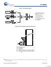
AutoStore
®
Operation
The CY14B256K stores data to nvSRAM using one of the three
storage operations:
1. Hardware store activated by HSB
2. Software store activated by an address sequence
3. AutoStore on device power down
AutoStore operation is a unique feature of QuantumTrap
technology and is enabled by default on the CY14B256K.
During normal operation, the device draws current from V
CC
to
charge a capacitor connected to the V
CAP
pin. This stored
charge is used by the chip to perform a single STORE operation.
If the voltage on the V
CC
pin drops below V
SWITCH
, the part
automatically disconnects the V
CAP
pin from V
CC
. A STORE
operation is initiated with power provided by the V
CAP
capacitor.
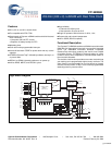
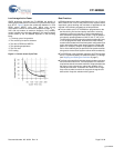
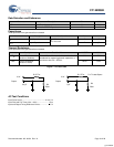
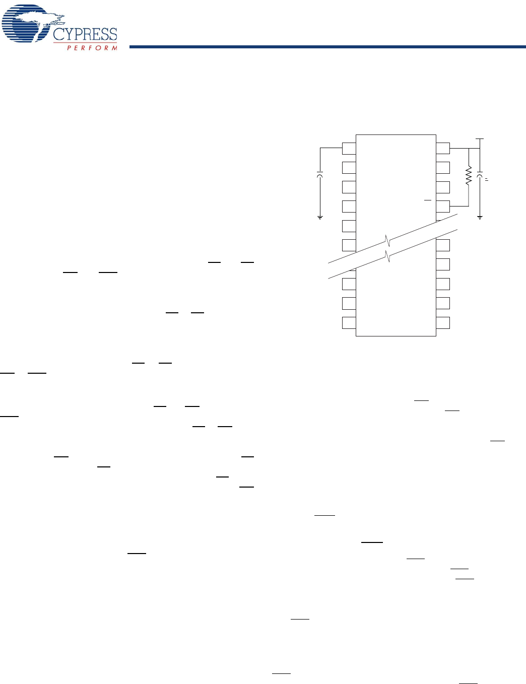
Figure 2 shows the proper connection of the storage capacitor
(V
CAP
) for automatic store operation. Refer to DC Electrical
Characteristics on page 15 for the size of the V
CAP
. The voltage
on the V
CAP
pin is driven to 5V
by a charge pump internal to the
chip. A pull up should be placed on WE
to hold it inactive during
power up. This pull up is only effective if the WE
signal is tri-state
during power up. Many MPUs tri-state their controls on power up.
Verify this when using the pull up. When the nvSRAM comes out
of power-on-recall, the MPU must be active or the WE
held
inactive until the MPU comes out of reset.
To reduce unnecessary nonvolatile stores, AutoStore and
Hardware Store operations are ignored unless at least one
WRITE operation has taken place since the most recent STORE
or RECALL cycle. Software initiated STORE cycles are
performed regardless of whether a WRITE operation has taken
place. The HSB
signal is monitored by the system to detect if an
AutoStore cycle is in progress.
Hardware STORE (HSB) Operation
The CY14B256K provides the HSB pin for controlling and
acknowledging the STORE operations. The HSB
pin is used to
request a hardware STORE cycle. When the HSB
pin is driven
low, the CY14B256K conditionally initiates a STORE operation
after t
DELAY
. An actual STORE cycle only begins if a WRITE to
the SRAM takes place since the last STORE or RECALL cycle.
The HSB pin also acts as an open drain driver that is internally
driven low to indicate a busy condition, while the STORE
(initiated by any means) is in progress. This pin is externally
pulled up if it is used to drive other inputs.
SRAM READ and WRITE operations, that are in progress when
HSB is driven low by any means, are given time to complete
before the STORE operation is initiated. After HSB
goes LOW,
the CY14B256K continues SRAM operations for t
DELAY
. During
Figure 2. AutoStore Mode
V
CC
V
CC
V
CAP
V
CAP
WE
10k Ohm
0.1 F
U
[+] Feedback