CY7C0430BV
CY7C0430CV
Document #: 38-06027 Rev. *B Page 26 of 37
address the entire memory array (depend on the value of
the mask register) and loop back to location 0. The
increment operation is second in priority to load operation.
3. Readback: the internal value of either the burst counter or
the mask register can be read out on the address lines when
CNTRD
or MKRD is LOW. Counter readback has higher
priority over mask register readback. A no-operation delay
cycle is experienced when readback operation is
performed. The address will be valid after t
CA2
(for counter
readback) or t
CM2
(for mask readback) from the following
port's clock rising edge. Address readback operation is
independent of the port's chip enables (CE
0
and CE
1
). If
address readback occurs while the port is enabled (chip
enables active), the data lines (I/Os) will be three-stated.
4. Hold operation: In order to hold the value of the address
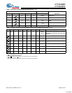
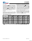
counter at certain address, all signals in Table 2 have to be
HIGH. This operation has the least priority. This operation
is useful in many applications where wait states are needed
or when address is available few cycles ahead of data.
The counter and mask register operations are totally
independent of port chip enables.
IEEE 1149.1 Serial Boundary Scan (JTAG) and
Memory Built-In-Self-Test (MBIST)
The CY7C0430BV and CY7C0430CV incorporate a serial
boundary scan test access port (TAP). This port is fully
compatible with IEEE Standard 1149.1-2001
[52]
. The TAP
operates using JEDEC standard 3.3V I/O logic levels. It is
composed of three input connections and one output
connection required by the test logic defined by the standard.
Memory BIST circuitry will also be controlled through the TAP
interface. All MBIST instructions are compliant to the JTAG
standard. An external clock (CLKBIST) is provided to allow the
user to run BIST at speeds up to 50 MHz. CLKBIST is multi-
plexed internally with the ports clocks during BIST operation.
Disabling the JTAG Feature
It is possible to operate the QuadPort DSE device without
using the JTAG feature. To disable the TAP controller, TCK
must be tied LOW (V
SS
) to prevent clocking of the device. TDI
and TMS are internally pulled up and may be unconnected.
They may alternately be connected to V
DD
through a pull-up
resistor. TDO should be left unconnected. CLKBIST must be
tied LOW to disable the MBIST. Upon power-up, the device will
come up in a reset state which will not interfere with the
operation of the device.
Test Access Port (TAP)–Test Clock (TCK)
The test clock is used only with the TAP controller. All inputs
are captured on the rising edge of TCK. All outputs are driven
from the falling edge of TCK.
Test Mode Select
The TMS input is used to give commands to the TAP controller
and is sampled on the rising edge of TCK. It is allowable to
leave this pin unconnected if the TAP is not used. The pin is
pulled up internally, resulting in a logic HIGH level.
Test Data-In (TDI)
The TDI pin is used to serially input information into the
registers and can be connected to the input of any of the
registers. The register between TDI and TDO is chosen by the
instruction that is loaded into the TAP instruction register. For
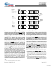
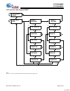
information on loading the instruction register, see the TAP
Controller State Diagram. TDI is internally pulled up and can
be unconnected if the TAP is unused in an application. TDI is
connected to the most significant bit (MSB) on any register.
Test Data Out (TDO)
The TDO output pin is used to serially clock data-out from the
registers. The output is active depending upon the current
state of the TAP state machine (see TAP Controller State
Diagram (FSM)). The output changes on the falling edge of
TCK. TDO is connected to the least significant bit (LSB) of any
register.
Performing a TAP Reset
A Reset is performed by forcing TMS HIGH (V
DD
) for five rising
edges of TCK. This RESET does not affect the operation of
the QuadPort DSE device and may be performed while the
device is operating. At power-up, the TAP is reset internally to
ensure that TDO comes up in a High-Z state.
TAP Registers
Registers are connected between the TDI and TDO pins and
allow data to be scanned into and out of the QuadPort DSE
device test circuitry. Only one register can be selected at a
time through the instruction registers. Data is serially loaded
into the TDI pin on the rising edge of TCK. Data is output on
the TDO pin on the falling edge of TCK.
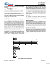
Instruction Register
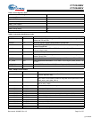
Four-bit instructions can be serially loaded into the instruction
register. This register is loaded when it is placed between the
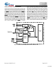
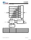
TDI and TDO pins as shown in the following JTAG/BIST
Controller diagram. Upon power-up, the instruction register is
loaded with the IDCODE instruction. It is also loaded with the
IDCODE instruction if the controller is placed in a reset state
as described in the previous section.
When the TAP controller is in the CaptureIR state, the two least
significant bits are loaded with a binary “01” pattern to allow for
fault isolation of the board level serial test path.
Bypass Register
To save time when serially shifting data through registers, it is
sometimes advantageous to skip certain devices. The bypass
register is a single-bit register that can be placed between TDI
and TDO pins. This allows data to be shifted through the
QuadPort DSE device with minimal delay. The bypass register
is set LOW (V
SS
) when the BYPASS instruction is executed.
Boundary Scan Register
The boundary scan register is connected to all the input and
output pins on the QuadPort DSE device. The boundary scan
register is loaded with the contents of the QuadPort DSE
device Input and Output ring when the TAP controller is in the
Capture-DR state and is then placed between the TDI and
TDO pins when the controller is moved to the Shift-DR state.
Note:
52.Master Reset will reset the JTAG controller.
[+] Feedback


