


CY7C0430BV
CY7C0430CV
Document #: 38-06027 Rev. *B Page 4 of 37
Addr.
Read
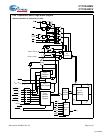
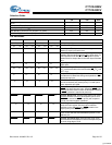
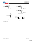
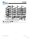
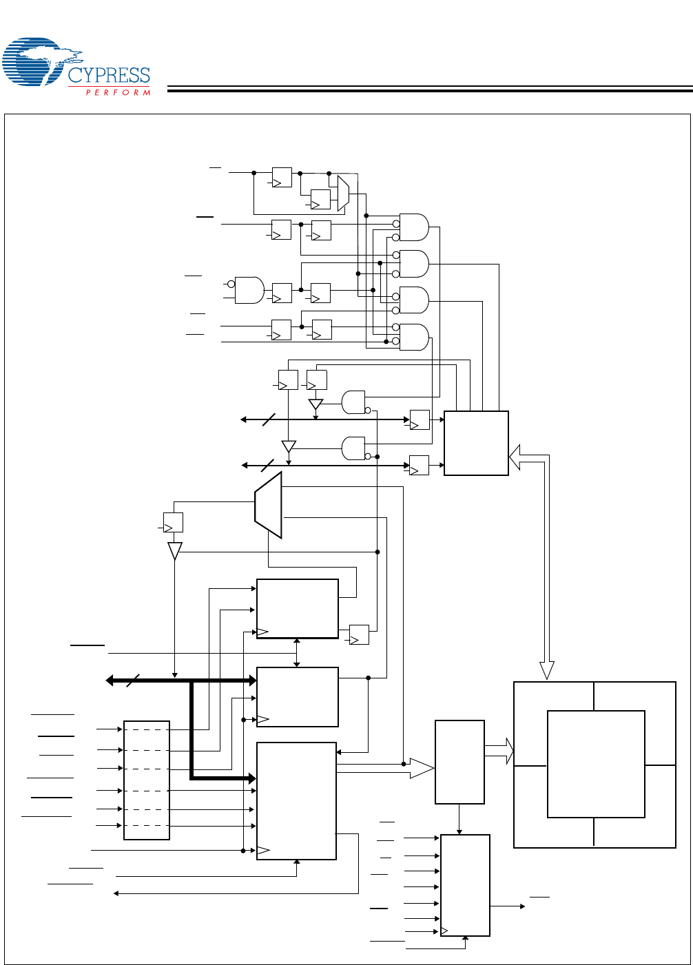
Port 1 Operation-Control Logic Block Diagram
R/W
P1
CE
0P1
CE
1P1
LB
P1
OE
P1
UB
P1
I/O
9P1
–I/O
17P1
I/O
0P1
–I/O
8P1
I/O
Control
Counter/
A
0P1
–A
15P1
CLK
P1
CNTLD
P1
CNTINC
P1
CNTRST
P1
16
9
9
MKLD
P1
CNTINT
P1
MKRD
P1
Mask Register
Port-1
Port 1
Port 1
64K × 18
QuadPort
DSE Array
P
or
t
1
Po
r
t 2
P
ort 4
P
ort 3
Address
Register
Readback
Register
Port 1
CNTRD
P1
Port 1
Address
Decode
Port 1
Interrupt
Logic
R/W
P1
CE
0P1
CE
1P1
OE
P1
INT
P1
CLK
P1
MRST
MRST
Priority
Decision
Logic
MRST
(Address Readback is independent of CEs)
W
LB
P1
UB
P1
[+] Feedback