


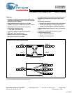
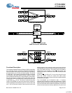
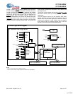
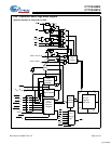
CY7C0430BV
CY7C0430CV
Document #: 38-06027 Rev. *B Page 8 of 37
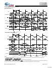
Maximum Ratings
(Above which the useful life may be impaired. For user guide-
lines, not tested.)
Storage Temperature ................................ –65
°C to + 150°C
Ambient Temperature with
Power Applied............................................–55
°C to + 125°C
Supply Voltage to Ground Potential .............. –0.5V to + 4.6V
DC Voltage Applied to
Outputs in High-Z State..........................–0.5V to V
CC
+ 0.5V
DC Input Voltage....................................–0.5V to V
CC
+ 0.5V
Output Current into Outputs (LOW)............................. 20 mA
Static Discharge Voltage...........................................> 2200V
Latch-up Current.....................................................> 200 mA
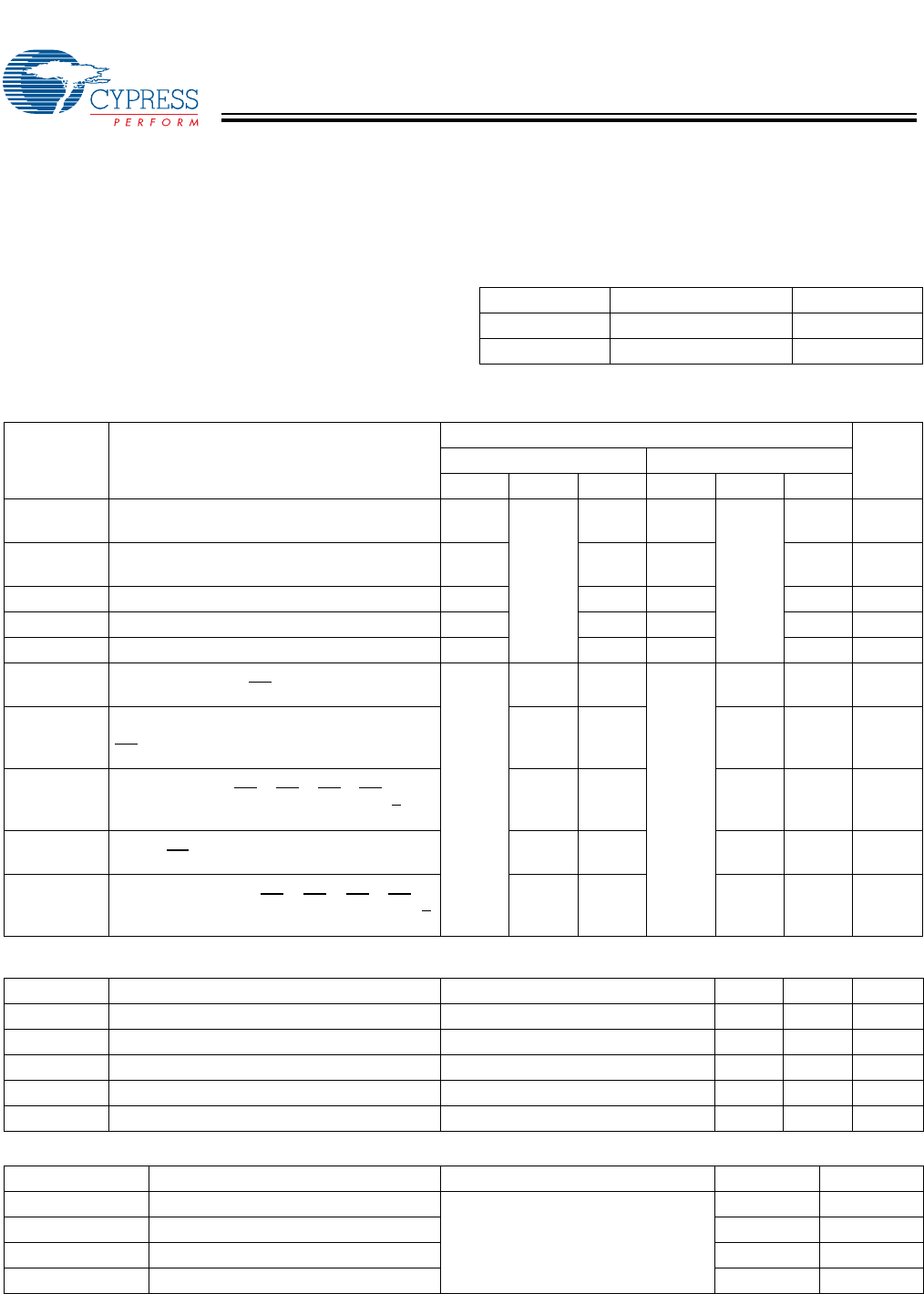
Operating Range
Range Ambient Temperature V
DD
Commercial 0°C to +70°C 3.3V ± 150 mV
Industrial –40
°C to +85°C 3.3V ± 150 mV
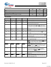
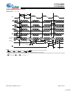
Electrical Characteristics Over the Operating Range
Parameter Description
Quadport DSE Family
Unit
–133 –100
Min. Typ. Max. Min. Typ. Max.
V
OH
Output HIGH Voltage
(V
CC
= Min., I
OH
= –4.0 mA)
2.4 2.4 V
V
OL
Output LOW Voltage
(V
CC
= Min., I
OH
= +4.0 mA)
0.4 0.4 V
V
IH
Input HIGH Voltage 2.0 2.0 V
V
IL
Input LOW Voltage 0.8 0.8 V
I
OZ
Output Leakage Current –10 10 –10 10 µA
I
CC
Operating Current (V
CC
= Max., I
OUT
= 0 mA)
Outputs Disabled, CE
= V
IL
, f = f
max
350 700 300 550 mA
I
SB1
Standby Current (four ports toggling at TTL
Levels,0 active)
CE
1-4
≥ V
IH
, f = f
MAX
80 200 60 150 mA
I
SB2
Standby Current (four ports toggling at TTL
Levels, 1 active)
CE
1
| CE
2
| CE
3
| CE
4
< V
IL
,
f = f
MAX
150 300 125 250 mA
I
SB3
Standby Current (four ports CMOS Level, 0
active)
CE
1–4
≥ V
IH
, f = 0
1.5 15 1.5 15 mA
I
SB4
Standby Current (four ports CMOS Level, 1
active and toggling) CE
1
| CE
2
| CE
3
| CE
4
<
V
IL
, f = f
MAX
110 290 85 240 mA
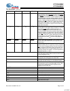
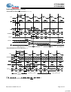
JTAG TAP Electrical Characteristics Over the Operating Range
Parameter Description Test Conditions Min. Max. Unit
V
OH1
Output HIGH Voltage I
OH
= −4.0 mA 2.4 V
V
OL1
Output LOW Voltage I
OL
= 4.0 mA 0.4 V
V
IH
Input HIGH Voltage 2.0 V
V
IL
Input LOW Voltage 0.8 V
I
X
Input Leakage Current GND ≤ V
I
≤ V
DD
–100 100 µA
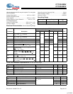
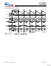
Capacitance
Parameter Description Test Conditions Max. Unit
C
IN
(All Pins) Input Capacitance T
A
= 25°C, f = 1 MHz,
V
CC
= 3.3V
10 pF
C
OUT
(All Pins) Output Capacitance 10 pF
C
IN
(CLK Pins) Input Capacitance 15 pF
C
OUT
(CLK Pins) Output Capacitance 15 pF
[+] Feedback