CY7C64013C
CY7C64113C
Document #: 38-08001 Rev. *B Page 19 of 51
9.0 General-Purpose I/O (GPIO) Ports
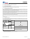
There are up to 32 GPIO pins (P0[7:0], P1[7:0], P2[7:0], and P3[7:0]) for the hardware interface. The number of GPIO pins
changes based on the package type of the chip. Each port can be configured as inputs with internal pull-ups, open drain outputs,
or traditional CMOS outputs. Port 3 offers a higher current drive, with typical current sink capability of 12 mA. The data for each
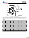
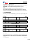
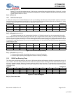
GPIO port is accessible through the data registers. Port data registers are shown in Figure 9-2 through Figure 9-5, and are set
to 1 on reset.
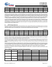
Port 0 Data ADDRESS 0x00
Port 1 Data ADDRESS 0x01
Port 2 Data ADDRESS 0x02
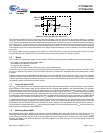
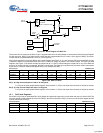
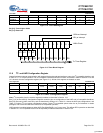
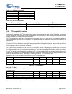
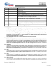
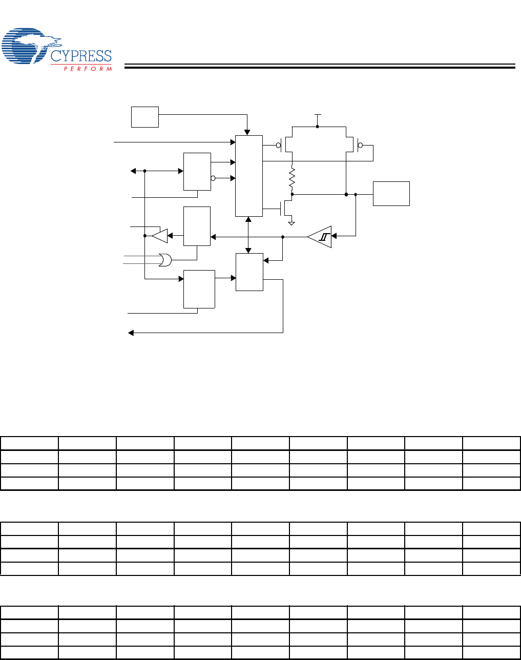
Figure 9-1. Block Diagram of a GPIO Pin
Bit # 76543210
Bit Name P0.7 P0.6 P0.5 P0.4 P0.3 P0.2 P0.1 P0.0
Read/Write R/W R/W R/W R/W R/W R/W R/W R/W
Reset 11111111
Figure 9-2. Port 0 Data
Bit # 76543210
Bit Name P1.7 P1.6 P1.5 P1.4 P1.3 P1.2 P1.1 P1.0
Read/Write R/W R/W R/W R/W R/W R/W R/W R/W
Reset 11111111
Figure 9-3. Port 1 Data
Bit # 76543210
Bit Name P2.7 P2.6 P2.5 P2.4 P2.3 P2.2 P2.1 P2.0
Read/Write R/W R/W R/W R/W R/W R/W R/W R/W
Reset 11111111
Figure 9-4. Port 2 Data
GPIO
V
CC
14 kΩ
GPIO
CFG
mode
2-bits
Data
Out
Latch
Internal
Data Bus
Port Read
Port Write
Interrupt
Enable
Control
Control
Interrupt
Controller
Q1
Q3*
Q2
*Port 0,1,2: Low I
sink
Port 3: High I
sink
Data
Interrupt
Latch
OE
Reg_Bit
STRB
Data
In
Latch
(Latch is Transparent
except in HAPI mode)
PIN
[+] Feedback


