CY7C64013C
CY7C64113C
Document #: 38-08001 Rev. *B Page 32 of 51
16.7 GPIO/HAPI Interrupt
Each of the GPIO pins can generate an interrupt, if enabled. The interrupt polarity can be programmed for each GPIO port as
part of the GPIO configuration. All of the GPIO pins share a single interrupt vector, which means the firmware needs to read the
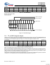
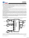
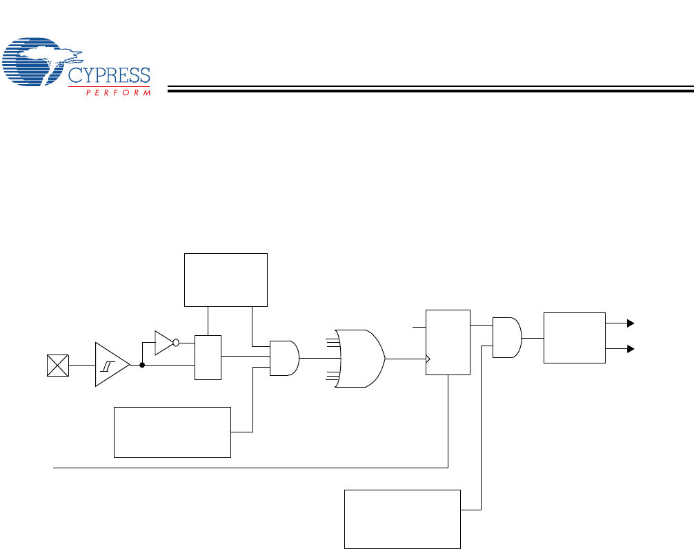
GPIO ports with enabled interrupts to determine which pin or pins caused an interrupt. A block diagram of the GPIO interrupt
logic is shown in Figure 16-4. Refer to Sections 9.1 and 9.2 for more information of setting GPIO interrupt polarity and enabling
individual GPIO interrupts.
If one port pin has triggered an interrupt, no other port pins can cause a GPIO interrupt until that port pin has returned to its inactive
(non-trigger) state or its corresponding port interrupt enable bit is cleared. The USB Controller does not assign interrupt priority
to different port pins and the Port Interrupt Enable Registers are not cleared during the interrupt acknowledge process.
When HAPI is enabled, the HAPI logic takes over the interrupt vector and blocks any interrupt from the GPIO bits, including
ports/bits not being used by HAPI. Operation of the HAPI interrupt is independent of the GPIO specific bit interrupt enables, and
is enabled or disabled only by bit 5 of the Global Interrupt Enable Register (Figure 16-1) when HAPI is enabled. The settings of
the GPIO bit interrupt enables on ports/bits not used by HAPI still effect the CMOS mode operation of those ports/bits. The effect
of modifying the interrupt bits while the Port Config bits are set to “10” is shown in Table 9-1. The events that generate HAPI
interrupts are described in Section 14.0.
16.8 I
2
C Interrupt
The I
2
C interrupt occurs after various events on the I
2
C-compatible bus to signal the need for firmware interaction. This generally
involves reading the I
2
C Status and Control Register (Figure 13-2) to determine the cause of the interrupt, loading/reading the
I
2
C Data Register as appropriate, and finally writing the Status and Control Register to initiate the subsequent transaction. The
interrupt indicates that status bits are stable and it is safe to read and write the I
2
C registers. Refer to Section 13.0 for details on
the I
2
C registers.
When enabled, the I
2
C-compatible state machines generate interrupts on completion of the following conditions. The referenced
bits are in the I
2
C Status and Control Register.
1. In slave receive mode, after the slave receives a byte of data: The Addr bit is set, if this is the first byte since a start or restart
signal was sent by the external master. Firmware must read or write the data register as necessary, then set the ACK, Xmit
MODE, and Continue/Busy bits appropriately for the next byte.
2. In slave receive mode, after a stop bit is detected: The Received Stop bit is set, if the stop bit follows a slave receive transaction
where the ACK bit was cleared to 0, no stop bit detection occurs.
3. In slave transmit mode, after the slave transmits a byte of data: The ACK bit indicates if the master that requested the byte
acknowledged the byte. If more bytes are to be sent, firmware writes the next byte into the Data Register and then sets the
Xmit MODE and Continue/Busy bits as required.
4. In master transmit mode, after the master sends a byte of data. Firmware should load the Data Register if necessary, and
set the Xmit MODE, MSTR MODE, and Continue/Busy bits appropriately. Clearing the MSTR MODE bit issues a stop signal
to the I
2
C-compatible bus and return to the idle state.
Figure 16-4. GPIO Interrupt Structure
Port
Register
OR Gate
GPIO Interrupt
Flip Flop
CLR
GPIO
Pin
1 = Enable
0 = Disable
Port Interrupt
Enable Register
1 = Enable
0 = Disable
Interrupt
Priority
Encoder
IRQout
Interrupt
Vector
D
Q
M
U
X
1
(1 input per
GPIO pin)
Global
GPIO Interrupt
Enable
(Bit 5, Register 0x20)
IRA
Configuration
[+] Feedback


