CY7C64013C
CY7C64113C
Document #: 38-08001 Rev. *B Page 27 of 51
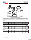
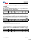
to the data register before setting the Continue bit. To prevent false ARB Lost signals, the Restart bit is cleared by hardware
during the restart sequence.
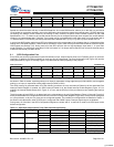
Bit 1 : Receive Stop
This bit is set when the slave is in receive mode and detects a stop bit on the bus. The Receive Stop bit is not set if the
firmware terminates the I
2
C transaction by not acknowledging the previous byte transmitted on the I
2
C-compatible bus,
e.g. in receive mode if firmware sets the Continue bit and clears the ACK bit.
Bit 0 : I
2
C Enable
Set this bit to override GPIO definition with I
2
C-compatible function on the two I
2
C-compatible pins. When this bit is cleared,
these pins are free to function as GPIOs. In I
2
C-compatible mode, the two pins operate in open drain mode, independent
of the GPIO configuration setting.
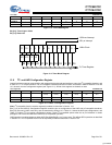
14.0 Hardware Assisted Parallel Interface (HAPI)
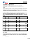
The CY7C64x13C processor provides a hardware assisted parallel interface for bus widths of 8, 16, or 24 bits, to accommodate
data transfer with an external microcontroller or similar device. Control bits for selecting the byte width are in the HAPI/I
2
C
Configuration Register (Figure 12-1), bits 1 and 0.
Signals are provided on Port 2 to control the HAPI interface. Table 14-1 describes these signals and the HAPI control bits in the
HAPI/I
2
C Configuration Register. Enabling HAPI causes the GPIO setting in the GPIO Configuration Register (0x08) to be
overridden. The Port 2 output pins are in CMOS output mode and Port 2 input pins are in input mode (open drain mode with Q3
OFF in Figure 9-1).
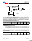
HAPI Read by External Device from CY7C64x13C:
In this case (see Figure 24-3), firmware writes data to the GPIO ports. If 16-bit or 24-bit transfers are being made, Port 0 should
be written last, since writes to Port 0 asserts the Data Ready bit and the DReady Pin to signal the external device that data is
available.
The external device then drives the OE
and CS pins active (LOW), which causes the HAPI data to be output on the port pins.
When OE
is returned HIGH (inactive), the HAPI/GPIO interrupt is generated. At that point, firmware can reload the HAPI latches
for the next output, again writing Port 0 last.
The Data Ready bit reads the opposite state from the external DReadyPin on pin P2[3]. If the DRDY Polarity bit is 0, DReadyPin
is active HIGH, and the Data Ready bit is active LOW.
HAPI Write by External Device to CY7C64x13C:
In this case (see Figure 24-4), the external device drives the STB
and CS pins active (LOW) when it drives new data onto the
port pins. When this happens, the internal latches become full, which causes the Latch Empty bit to be deasserted. When STB
is returned HIGH (inactive), the HAPI/GPIO interrupt is generated. Firmware then reads the parallel ports to empty the HAPI
latches. If 16-bit or 24-bit transfers are being made, Port 0 should be read last because reads from Port 0 assert the Latch Empty
bit and the LatEmptyPin to signal the external device for more data.
The Latch Empty bit reads the opposite state from the external LatEmptyPin on pin P2[2]. If the LEMPTY Polarity bit is 0,
LatEmptyPin is active HIGH, and the Latch Empty bit is active LOW.
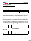
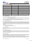
Table 14-1. Port 2 Pin and HAPI Configuration Bit Definitions
Pin Name Direction Description (Port 2 Pin)
P2[2] LatEmptyPin Out Ready for more input data from external interface.
P2[3] DReadyPin Out Output data ready for external interface.
P2[4] STB
In Strobe signal for latching incoming data.
P2[5] OE
In Output Enable, causes chip to output data.
P2[6] CS
In Chip Select (Gates STB and OE).
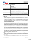
Bit Name R/W Description (HAPI/I
2
C Configuration Register)
2 Data Ready R Asserted after firmware writes data to Port 0, until OE
driven LOW.
3 Latch Empty R Asserted after firmware reads data from Port 0, until STB driven LOW.
4 DRDY Polarity R/W Determines polarity of Data Ready bit and DReadyPin:
If 0, Data Ready is active LOW, DReadyPin is active HIGH.
If 1, Data Ready is active HIGH, DReadyPin is active LOW.
5 LEMPTY Polarity R/W Determines polarity of Latch Empty bit and LatEmptyPin:
If 0, Latch Empty is active LOW, LatEmptyPin is active HIGH.
If 1, Latch Empty is active HIGH, LatEmptyPin is active LOW.
[+] Feedback


