CY7C64013C
CY7C64113C
Document #: 38-08001 Rev. *B Page 23 of 51
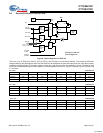
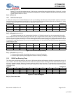
Bit [4..0]: Isink [x] (x= 0..4)
Writing all ‘0’s to the Isink register causes 1/5 of the max current to flow through the DAC I/O pin. Writing all ‘1’s to the
Isink register provides the maximum current flow through the pin. The other 14 states of the DAC sink current are evenly
spaced between these two values.
Bit [7..5]: Reserved
10.2 DAC Port Interrupts
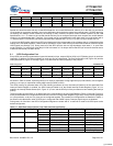
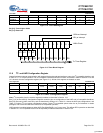
A DAC port interrupt can be enabled/disabled for each pin individually. The DAC Port Interrupt Enable register provides this
feature with an interrupt enable bit for each DAC I/O pin.All of the DAC Port Interrupt Enable register bits are cleared to ‘0’ during
a reset. All DAC pins share a common interrupt, as explained in Section 16.6.
DAC Port Interrupt ADDRESS 0x31
Bit [7..0]: Enable bit x (x= 0..2, 7)
1= Enables interrupts from the corresponding bit position; 0= Disables interrupts from the corresponding bit position
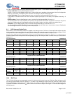
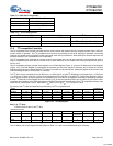
As an additional benefit, the interrupt polarity for each DAC pin is programmable with the DAC Port Interrupt Polarity register.
Writing a ‘0’ to a bit selects negative polarity (falling edge) that causes an interrupt (if enabled) if a falling edge transition occurs
on the corresponding input pin. Writing a ‘1’ to a bit in this register selects positive polarity (rising edge) that causes an interrupt
(if enabled) if a rising edge transition occurs on the corresponding input pin. All of the DAC Port Interrupt Polarity register bits are
cleared during a reset.
DAC Port Interrupt Polarity ADDRESS 0x32
Bit [7..0]: Enable bit x (x= 0..2, 7)
1= Selects positive polarity (rising edge) that causes an interrupt (if enabled);
0= Selects negative polarity (falling edge) that causes an interrupt (if enabled)
11.0 12-Bit Free-Running Timer
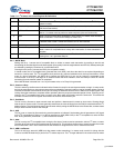
The 12-bit timer provides two interrupts (128-µs and 1.024-ms) and allows the firmware to directly time events that are up to 4
ms in duration. The lower 8 bits of the timer can be read directly by the firmware. Reading the lower 8 bits latches the upper 4
bits into a temporary register. When the firmware reads the upper 4 bits of the timer, it is accessing the count stored in the
temporary register. The effect of this logic is to ensure a stable 12-bit timer value can be read, even when the two reads are
separated in time.
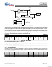
Timer LSB ADDRESS 0x24
Bit [7:0]: Timer lower 8 bits
Bit # 76543210
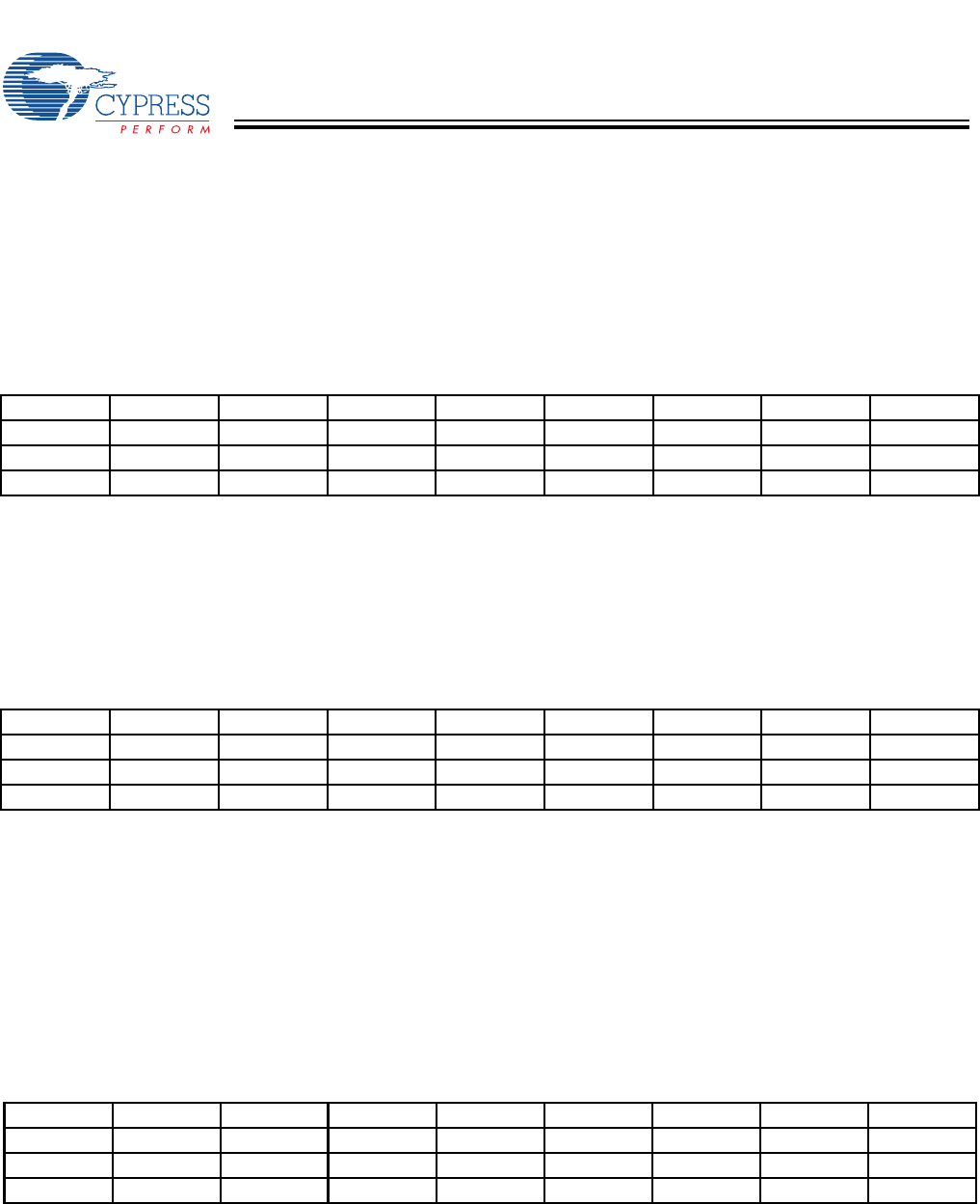
Bit Name Enable Bit 7 Reserved Reserved Reserved Reserved Enable Bit 2 Enable Bit 1 Enable Bit 0
Read/Write WWWWWWWW
Reset 00000000
Figure 10-4. DAC Port Interrupt Enable
Bit # 76543210
Bit Name Enable Bit 7 Reserved Reserved Reserved Reserved Enable Bit 2 Enable Bit 1 Enable Bit 0
Read/Write WWWWWWWW
Reset 00000000
Figure 10-5. DAC Port Interrupt Polarity
Bit # 76543210
Bit Name Timer Bit 7 Timer Bit 6 Timer Bit 5 Timer Bit 4 Timer Bit 3 Timer Bit 2 Timer Bit 1 Timer Bit 0
Read/Write RRRRRRRR
Reset 00000000
Figure 11-1. Timer LSB Register
[+] Feedback


