AN42 APPLICATION NOTE
14
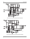
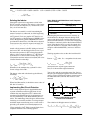
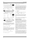
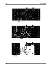
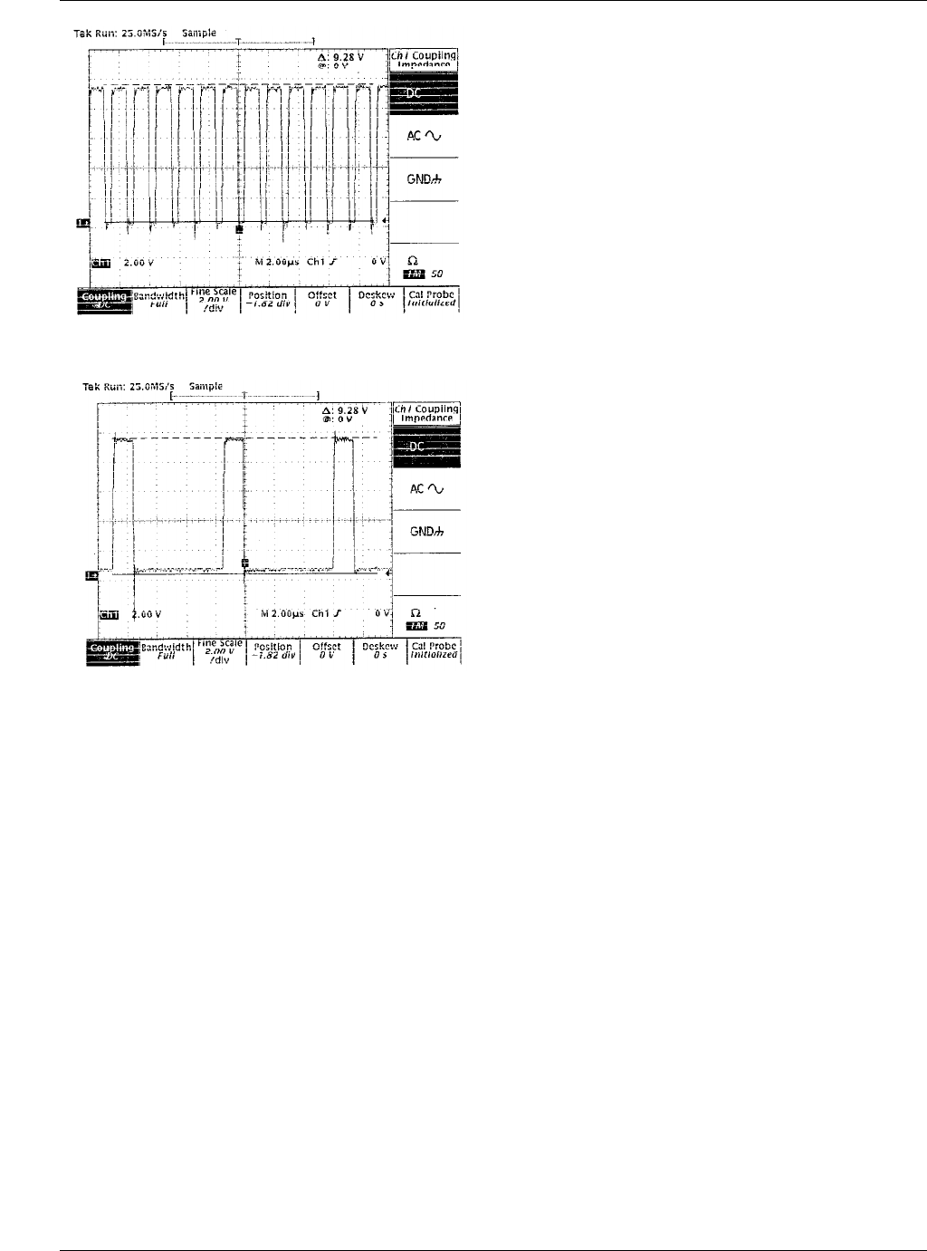
Figure 14A. V
CCQP
Output Waveform for Normal
Operation Condition with V
out
= 3.3V@10A
Figure 14B. V
CCQP
Output Waveform for
Output Shorted to Ground
The Schottky diode has a power dissipation consideration
during the short circuit condition. During normal operation,
the diode dissipates power when the power MOSFET is off.
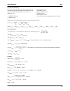
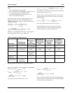
The power dissipation is given by:
In short circuit mode, the duty cycle is dramatically reduced
to approximately 20%. The forward current during a short
circuit condition decays exponentially through the inductor.
The power dissipated on the diode during the short circuit
condition, is approximated by:
Thus for the Schottky diode, the thermal dissipation during
a short circuit is greatly magnified and requires that the
thermal dissipation of the diode be properly managed by the
appropriate choice of a heat sink. In order to protect the
Schottky from being destroyed in the event of a short, we
should limit the junction temperature to less than 130°C.
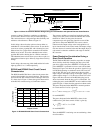
Using the equation for maximum junction temperature,
we can arrive at the thermal resistance required below:
Assuming that the ambient temperature is 50°C, we get:
Thus we need to provide for a heat sink that will give the
Schottky diode a thermal resistance of at least 16°C/W or
lower in order to protect the device during an indefinite
short.
In summary, with proper heat sink, the Schottky diode is not
being over stressed during a short circuit condition.
Schottky Diode Selection
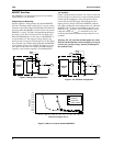
The application circuits of Figures 3, 4, and 5 show two
Schottky diodes, DS1 and DS2. In synchronous mode, DS1
is used in parallel with M3 to prevent the lossy diode in the
FET from turning on. In non-synchronous mode, DS1 is
used as a flyback diode to provide a constant current path for
the inductor when M1 is turned off.
The Schottky diode DS2 serves a dual purpose. As config-
ured in Figures 3, 4, and 5, DS2 allows the VCCQP pin on
the RC5040 to be bootstrapped up to 9V using capacitor
C12. When the lower MOSFET M3 is turned on, one side of
capacitor C12 is connected to ground while the other side of
the capacitor is being charged up to voltage VIN – VD
through DS2. The voltage that is then applied to the gate of
the MOSFET is VCCQP – VSAT, or typically around 9V.
DS2 also provides correct sequencing of the various supply
voltages by assuring that VCCQP is not enabled before the
other supplies.
A vital selection criteria for DS1 and DS2 is that they exhibit
a very low forward voltage drop, as this parameter can
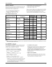
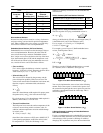
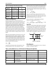
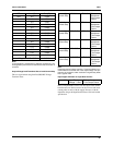
directly affect the regulator efficiency. Table 10 lists several
suitable Schottky diodes. Note that the MBR2015CTL has a
very low forward voltage drop. This diode is ideal for appli-
cations where output voltages less than 2.8V are required.
P
D Diode,
I
F
V
F
× 1 DutyCycle–( )× = =
14.5 0.5V× 1 0.62–( ) 2.75W=×
I
F ending,
I
sc
e
1
L R⁄
-----------–
× 20A e
1.5us
1.3us
-------------–
× 7.9A≈==
I
F ave,
20A 7.9A+( ) 2⁄ 14A≈ ≈
P
D Diode,
I
F ave,
V
F
× 1 DutyCycle–( )× = =
14 0.45× 0.8× 5W≈
P
D
T
J max( )
T
A
–
R
ΘJA
--------------------------------=
R
ΘJA
T
J max( )
T
A
–
P
D
--------------------------------
130 50–
5
--------------------- 16°C W⁄= = =


