AN42 APPLICATION NOTE
4
High Current Output Drivers
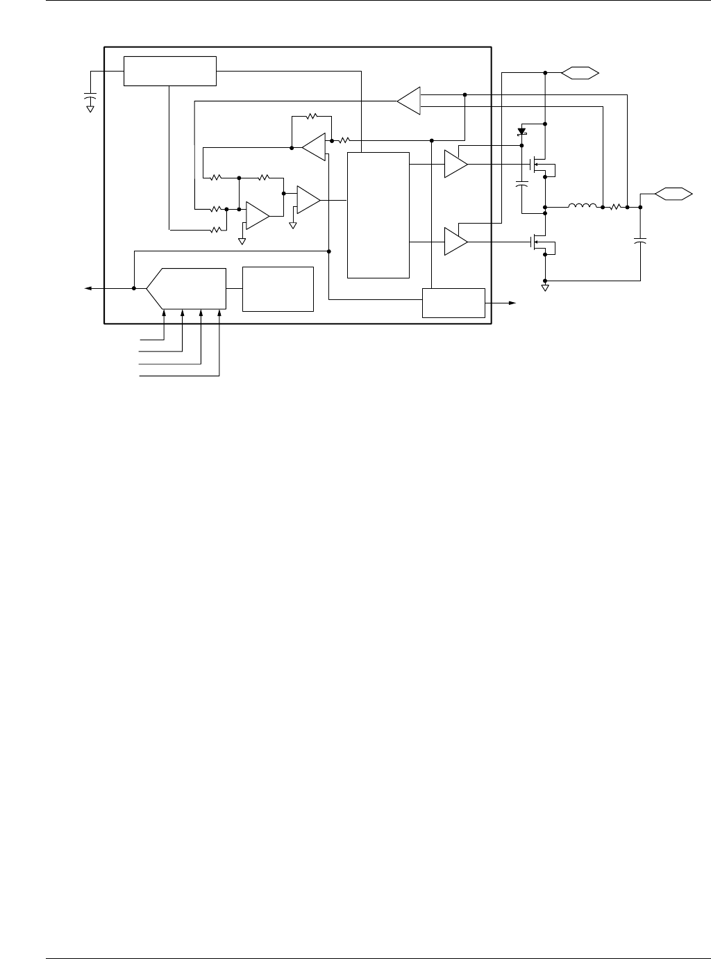
The RC5040 contains two identical high current output
drivers that use high speed bipolar transistors in a push-pull
configuration. Each driver is capable of delivering 1A of cur-
rent in less than 100ns. Each driver’s power and ground are
separated from the chip power and ground for additional
switching noise immunity. The HIDRV driver’s power sup-
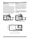
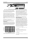
ply, VCCQP, is boot-strapped from a flying capacitor as
illustrated in Figure 3. Using this configuration, C12 is
charged from VCC via the Schottky diode DS2 and boosted
when the FET is turned on. This scheme provides a VCCQP
voltage equal to 2•VCC – VDS(DS2), or approximately 9.5V
when VCC = 5V. This voltage is sufficient to provide the 9V
gate drive to the MOSFET that is required to achieve a low
R
DS(ON). Since the low side synchronous FET is referenced to
ground (see Figure 4), boosting the gate drive voltage is not
needed and the VCCP power pin can be tied to VCC.
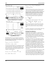
Refer to Typical Operating Characteristics of the RC5040
data sheet for a full load VCCQP waveform.
Internal Voltage Reference
The reference used in the RC5040 is a precision band-gap
voltage reference, with internal resistors precisely trimmed
to provide a near zero temperature coefficient, TC. Added to
the reference voltage is the output from a 4-bit DAC. The
DAC is provided meet Pentium Pro specifications, requiring
a programmable converter output via a 4-bit voltage identifi-
cation (VID) code. This code scales the output voltage from
2.0V (no CPU) to 3.5V in 100mV increments. To guarantee
stable operation under all loads, a 10KΩ pull-up resistor and
0.1µF of decoupling capacitance should be connected to the
VREF pin. No load should be imposed on this pin.
Power Good (PWRGD)
The RC5040 and RC5042 Power Good function has been
designed according to Intel’s Pentium Pro DC-DC converter
specification. The Power Good function provides a constant
voltage monitor on the VFB pin. The internal circuitry of the
converter compares the VFB signal to the VREF voltage and
outputs an active-low interrupt signal to the CPU when the
power supply voltage exceeds ±7% of its nominal setpoint.
The Power Good flag provides no other control function to
the RC5040.
Output Enable (OUTEN)
Intel specifications state that the DC-DC converter should
accept an open collector signal for controlling the output
voltage. A logic LOW for this signal disables the output volt-
age. When disabled, the PWRGD output is in the low state.
This feature is available for the RC5040 only.
Upgrade Present (UP#)
Intel specifications state that the DC-DC converter must
accept an open collector signal that indicates the presence of
an upgrade processor. The typical state is high (for a stan-
dard P6 processor). When the signal is low or in theground
state (for the OverDrive processor), the output voltage must
be disabled unless the converter can supply the OverDrive
processor’s power requirements. When disabled, the
PWRGD output must be in the low state. Because the
RC5040 and RC5042 can supply the OverDrive processor
requirements, the UP# signal is not required.
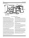
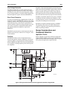
Main Control Loop
Figure 2. RC5040 Block Diagram
DIGITAL
CONTROL
–
+
1.24V
REFERENCE
4-BIT
DAC
65-5040-01
POWER
GOOD
OSCILLATOR
RC5040
PWRGD
VID0
VID1
VID2
VID3
–
+
–
+
–
+
VIN
VO
VREF
+5V


