APPLICATION NOTE AN42
19
Guidelines for Debugging and
Performance Evaluations
Debugging Your First Design Implementation
Use the following procedure to help you debug your design
implementation:
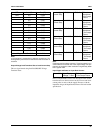
1. Note the VID pins settings. They tell you what voltage is
to be expected.
2. Do not connect any load to the circuit. While monitoring
the output voltage, apply power to the part with current
limiting at the power supply. Do this to make sure that
no catastrophic shorts occur.
3. Ιf proper voltage is not achieved, follow the procedures
in the Troubleshooting section.
4. After there is proper voltage, increase the current limit-
ing of the power supply to 16A.
5. Apply load at 1A increments; an active load (HP6060B
or equivalent) is suggested.
6. In case of poor regulation, refer to the procedures in the
Troubleshooting section.
Troubleshooting
1. If no voltage is registered at the output and the circuit is
not drawing current, look for openings in the connec-
tions. Check the circuitry versus the schematic, and the
power supply pins at the device to ascertain that volt-
age(s) had been applied.
2. If no voltage is registered at the output and the circuit is
drawing excessive current (>100mA) with no load,
check for possible shorts. Trace the path of the excessive
current to determine if the controller is at fault or if the
excessive current is due to peripheral components.
3. If the output voltage comes near to, but is not, what is
expected, check the VID inputs at the device pins. The
part is factory set to correspond to the VID inputs.


